Photoelectric conversion element

a conversion element and photoelectric technology, applied in the field of photoelectric conversion elements, can solve the problems of low photoelectric conversion efficiency, and low efficiency of two-step light absorption through quantum levels (including superlattice minibands) to achieve the effect of increasing the photoelectric conversion efficiency of a photoelectric conversion elemen

Active Publication Date: 2017-03-21
SHARP KK +1
View PDF2 Cites 1 Cited by
  • Summary
  • Abstract
  • Description
  • Claims
  • Application Information

AI Technical Summary

Benefits of technology

[0008]An embodiment of the present disclosure provides a technique for increasing the photoelectric conversion efficiency of a photoelectric conversion element.

Problems solved by technology

At present, in a solar cell including a quantum dot layer, the extraction efficiency of carriers generated in the quantum dot layer is very low and therefore the photoelectric conversion efficiency is low.
A cause of this is probably the fact that the efficiency of two-step light absorption through quantum levels (including a superlattice miniband) is low.
Therefore, there is a problem in that the second light absorption is insufficient, although the first light absorption is sufficient.
However, the patent document does not disclose that incident light is converted into light with a wavelength corresponding to an optical transition from a quantum level corresponding to the second light absorption to a conduction band using a wavelength conversion material in order to increase the photoelectric conversion efficiency.

Method used


Image

  • Photoelectric conversion element
  • Photoelectric conversion element
  • Photoelectric conversion element

Examples


embodiment

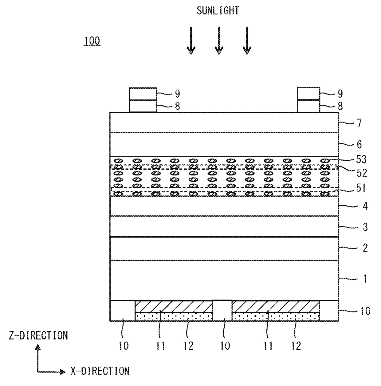
[0040]The photoelectric conversion element and a solar cell are described below in detail with reference to the attached drawings. In the drawings, the same reference numerals denote the same components or corresponding components. Dimensions such as length, width, thickness, and depth are appropriately modified for the clarification and simplification of the drawings and do not express actual dimensions.

[0041]Terms used in this specification are simply described below. The terms are used to describe a configuration in this embodiment and do not limit the present disclosure.

[0042]The term “superlattice semiconductor layer” refers to a layer having a superlattice structure composed of barrier sub-layers and quantum sub-layers alternately stacked. The barrier sub-layers and the quantum sub-layers are made of a compound semiconductor material. The barrier sub-layers are higher in band gap energy than the quantum sub-layers.

[0043]The term “quantum sub-layers” includes quantum dot sub-la...

experiment example 1

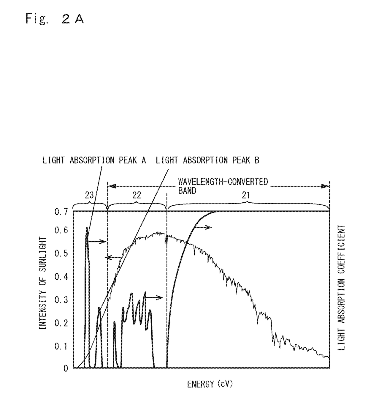
[0111]A simulation experiment below was performed using the solar cell 100 manufactured in the above embodiment.

experiment example 2

[0126]In Experiment Example 2, simulation was performed by substantially the same method as that described in Experiment Example 1 except that the height of quantum dots 53 was changed. That is, the height of the quantum dots 53 was changed from the conditions described in Experiment Example 1.

[0127]As is the case with Experiment Example 1, in a superlattice semiconductor layer 5, a base semiconductor material used to form barrier sub-layers 51 was gallium arsenide (GaAs) and a material used to form quantum dots 53 was Indium arsenide (InAs). In this experiment example, the base semiconductor material was GaAs and the material used to form the quantum dots 53 was InAs. However, a mixed crystal material such as InGaAs or a different semiconductor material may be used.

[0128]In the superlattice semiconductor layer 5, the quantum dots 53 were lens-shaped and each included a wetting layer with a thickness of about 0.5 nm, the diameter of the quantum dots 53 in the in-plane direction was ...


PUM


Abstract

A photoelectric conversion element includes a superlattice semiconductor layer including barrier sub-layers and quantum sub-layers (quantum dot sub-layers) alternately stacked and also includes a wavelength conversion layer containing a wavelength conversion material converting the wavelength of incident light. The wavelength conversion layer converts incident light into light with a wavelength corresponding to an optical transition from a quantum level of the conduction band of the superlattice semiconductor layer to a continuum level of the conduction band.

Description

BACKGROUND[0001]1. Field[0002]The present disclosure relates to a photoelectric conversion element.[0003]2. Description of the Related Art[0004]A great deal of research and development has been carried out on solar cells for the purpose of increasing the photoelectric conversion efficiency using light in a wider wavelength range. For example, Physical Review Letters, vol. 97, p. 247701, 2006 (hereinafter referred to as the “non-patent document”) proposes a solar cell that can photoexcite electrons in two steps to use light with a long wavelength in such a manner that a superlattice miniband is formed between the valence band and conduction band of a base material.[0005]The solar cell has quantum dots as disclosed in the non-patent document and has a structure in which a quantum dot layer having quantum dots is inserted in a compound solar cell. Such a structure enables the absorption of light in an unused wavelength range (the absorption of a photon with an energy less than the band...

Claims


Application Information

Patent Timeline
Patent Type & Authority Patents(United States)
IPC IPC(8): H01L29/06H01L31/055H01L31/0232H01L31/072H01L31/0352H01L31/109H01L31/054
CPCH01L31/035236H01L31/02322H01L31/02327H01L31/055H01L31/0547H01L31/072H01L31/109Y02E10/52H01L31/035218
Inventor YOSHIKAWA, HIROFUMIIZUMI, MAKOTOARAKAWA, YASUHIKO
Owner SHARP KK
Why Eureka
Try Eureka