Avalanche diode having reduced dark current and method for its manufacture

a diode and diode technology, applied in the field of avalanche diodes, to achieve the effect of reducing dark curren

Active Publication Date: 2017-08-29
NAT TECH & ENG SOLUTIONS OF SANDIA LLC
View PDF9 Cites 34 Cited by
  • Summary
  • Abstract
  • Description
  • Claims
  • Application Information

AI Technical Summary

Benefits of technology

[0012]We have found a way to apply this known phenomenon to reduce dark current in avalanche photodiodes. More specifically, we have developed a design for an avalanche diode and a fabricatio...

Problems solved by technology

This has been attributed to the four percent lattice mismatch between germanium and silicon.
In germanium/silicon avalanche diodes, the presence of thread...

Method used


Image

  • Avalanche diode having reduced dark current and method for its manufacture
  • Avalanche diode having reduced dark current and method for its manufacture
  • Avalanche diode having reduced dark current and method for its manufacture

Examples


Embodiment Construction

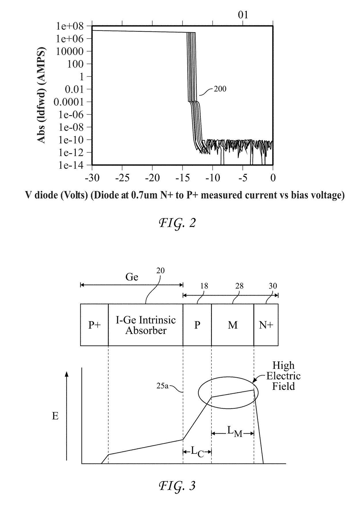
[0028]The following discussion commences with a review of the avalanche photodiode (APD) structure and variations thereof that were described in the above-cited U.S. patent application Ser. No. 13 / 915,369. We will then describe an example of a design modification that incorporates aspect ratio trapping for improved performance.

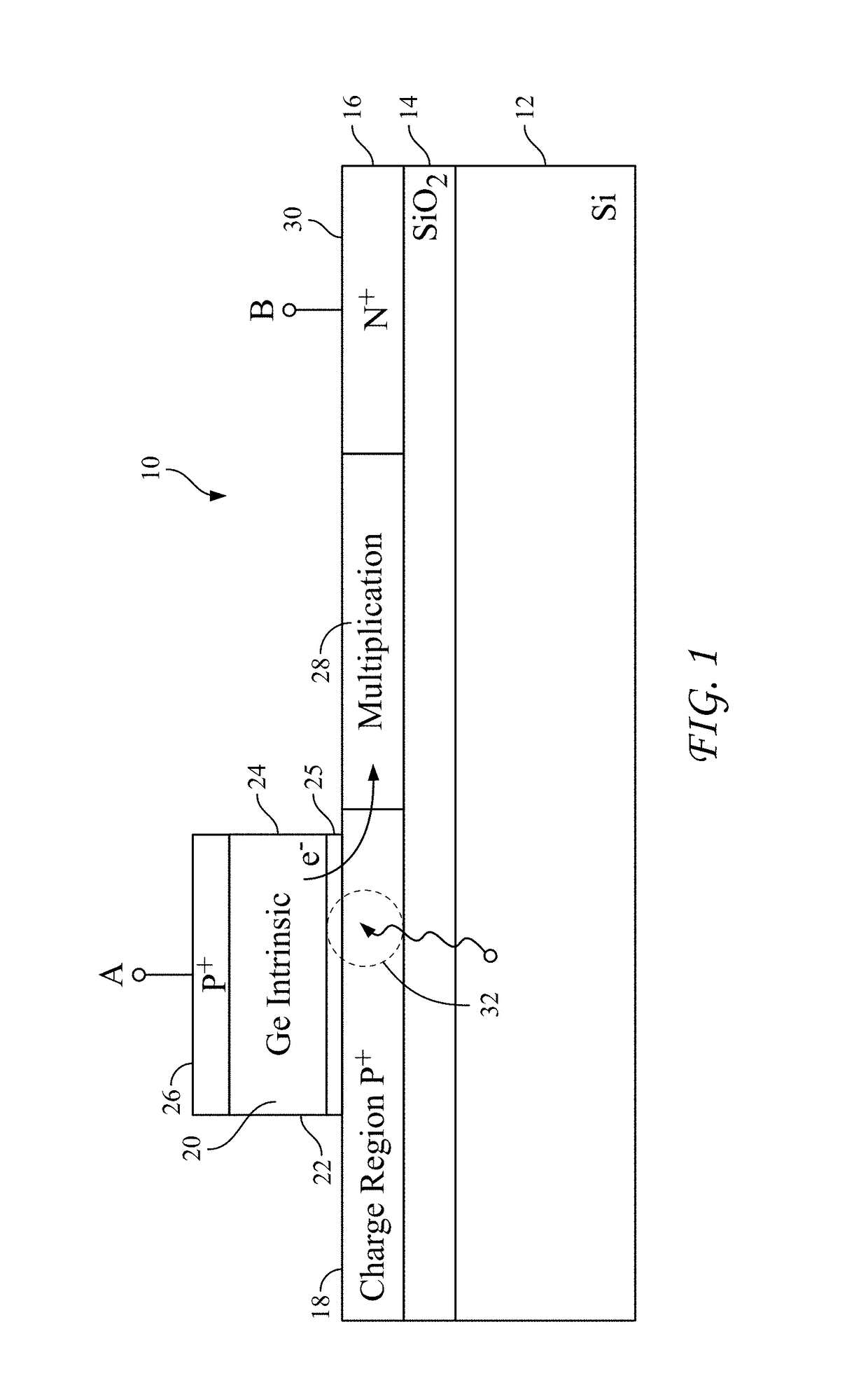
[0029]FIG. 1 depicts a side view of a device 10, such as an APD. The device 10 includes a silicon substrate 12, an insulating layer 14 and a relatively thin (e.g., less than one micrometer in thickness) silicon surface layer 16. The insulating layer 14 is made from silicon dioxide (SiO2) for example. The substrate 12 and layers 14, 16 are jointly referred to as a silicon-on-insulator or SOI structure or “platform”.

[0030]The silicon surface layer 16 comprises a region 18 formed within a predetermined area of the layer 16. In the example shown in FIG. 1, region 18 comprises a p-type silicon “charge” region. It should be understood that the device 10 includes a c...


PUM


Abstract

An avalanche diode includes an absorption region in a germanium body epitaxially grown on a silicon body including a multiplication region. Aspect-ratio trapping is used to suppress dislocation growth in the vicinity of the absorption region.

Description

CROSS-REFERENCE TO RELATED APPLICATIONS[0001]This application is a continuation-in-part of the commonly owned U.S. patent application Ser. No. 13 / 915,369 filed on Jun. 11, 2013 under the title “Two-Dimensional APDs and SPADs and Related Methods”, the entirety of which is hereby incorporated herein by reference.GOVERNMENT LICENSE RIGHTS[0002]This invention was developed under Contract DE-AC04-94AL85000 between Sandia Corporation and the U.S. Department of Energy. The U.S. Government has certain rights in this invention.FIELD OF THE INVENTION[0003]The invention relates to avalanche photodiodes and methods of their manufacture. The invention relates more particularly to avalanche diodes realized in the germanium-silicon materials system.ART BACKGROUND[0004]Avalanche photodiodes (APDs) have applications as very sensitive detectors of optical signals. When operated with a reverse voltage greater than its breakdown voltage, a mode of operation often referred to as “Geiger mode”, an avalan...

Claims


Application Information

Patent Timeline
IPC IPC(8): G01J1/04H01L31/107H01L31/0232H01L31/028
CPCH01L31/1075H01L31/02327H01L31/028G02B6/12004H01L31/035281G02B2006/12061G02B2006/12123Y02E10/547
Inventor DAVIDS, PAULSTARBUCK, ANDREW LEEPOMERENE, ANDREW T. S.
Owner NAT TECH & ENG SOLUTIONS OF SANDIA LLC
Why Eureka
Try Eureka