Method for manufacturing bonded SOI wafer

a technology of bonded soi and bonded film, which is applied in the manufacturing of semiconductor/solid-state devices, basic electric elements, electric devices, etc., can solve the problems of large surface roughness compared to mirror surfaces, deterioration of film, and damaged layers, so as to reduce heat treatment and suppress the variation of the radial distribution of buried oxide film thickness.

Active Publication Date: 2017-10-17
SHIN-ETSU HANDOTAI CO LTD
View PDF34 Cites 2 Cited by
  • Summary
  • Abstract
  • Description
  • Claims
  • Application Information

AI Technical Summary

Benefits of technology

[0036]The inventive method for manufacturing an SOI wafer can suppress variation of a radial distribution of a buried oxide film thickness caused by a reducing heat treatment performed after delaminating an SOI layer.

Problems solved by technology

In case of manufacturing the SOI wafer by the ion-implantation delamination method, however, the SOI wafer surface after delamination has a damaged layer caused by the ion-implantation, and has a larger surface roughness compared to a mirror surface of a silicon wafer on a normal product level.
When the SOI layer is subjected to polishing including a machining element, however, since the polishing stock removal is not uniform, there arises a problem of deteriorating film thickness uniformity of the SOI layer achieved by implantation of hydrogen ions or the like and delamination.

Method used


Image

  • Method for manufacturing bonded SOI wafer
  • Method for manufacturing bonded SOI wafer
  • Method for manufacturing bonded SOI wafer

Examples


example

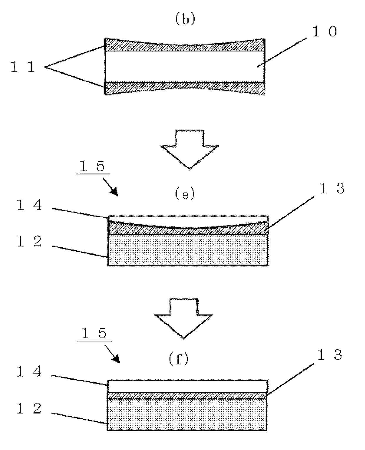
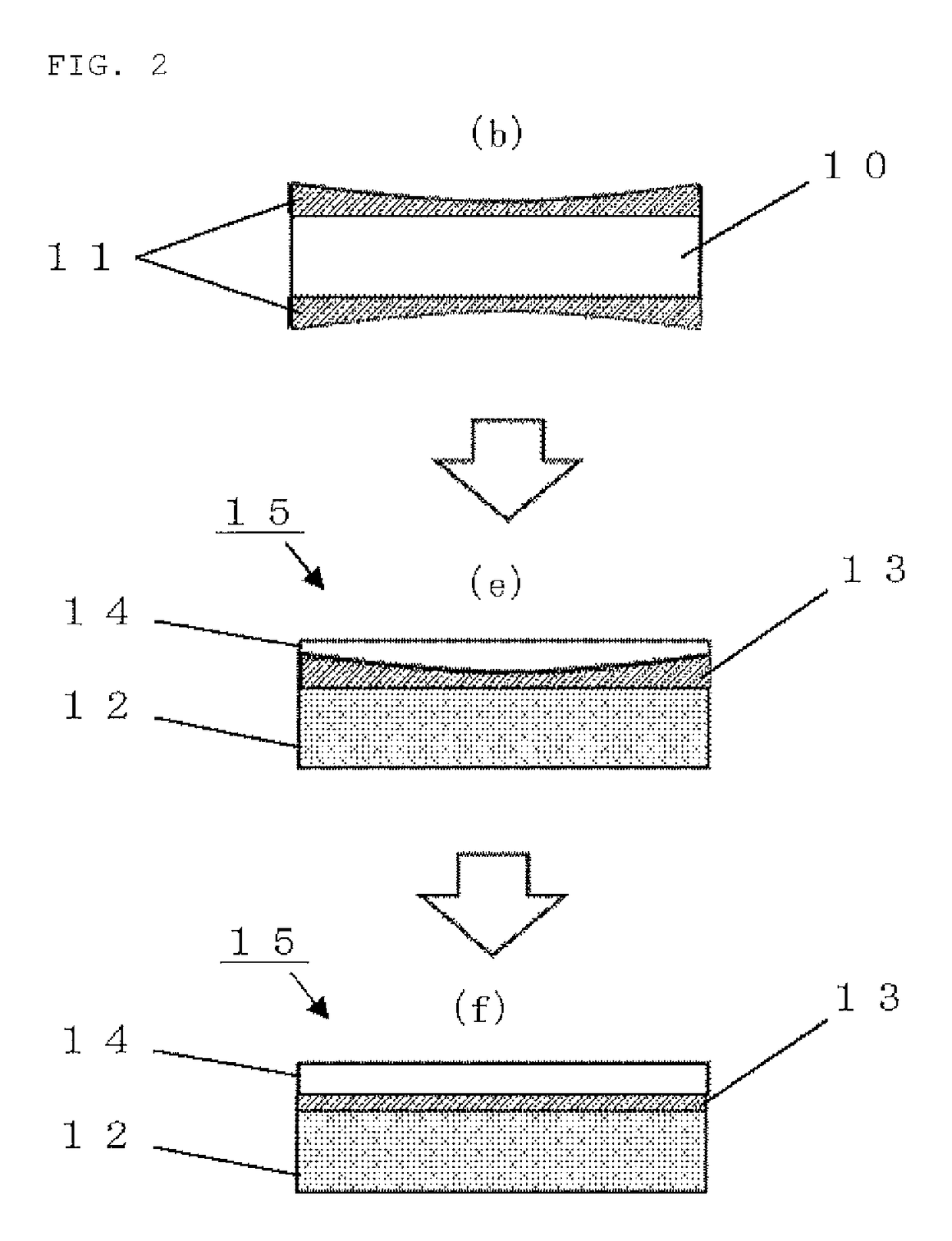
[0070]Only to a bond wafer with a diameter of 300 mm made of silicon single crystal, a silicon oxide film (the silicon oxide film to be a BOX film after delamination) was prepared with a thickness of 30 nm ((b) of FIG. 1), and then hydrogen ion-implantation was performed ((c) of FIG. 1).

[0071]A silicon oxide film was formed by using a batch type heat treatment furnace, and introducing oxygen gas during temperature-rising of 900° C. to 950° C. and during isothermal-holding at 950° C., thereby performing temperature-rise oxidation of dry oxidation. In order to enhance the effect of the temperature-rise oxidation, the temperature-rise rate during the temperature-rising of 900° C. to 950° C. was set to 1° C. / min. (It is to be noted that the wafer was put to the oxidation furnace at a temperature of 600° C., and the temperature-rise rate from 600° C. to 900° C. was set to 5° C. / min).

[0072]The radial range in the radial distribution of the silicon oxide film after the temperature-rise oxi...


PUM

PropertyMeasurementUnit
thicknessaaaaaaaaaa
thicknessaaaaaaaaaa
diameteraaaaaaaaaa

Abstract

The present invention is a method for manufacturing a bonded SOI wafer including: performing a thermal oxidation treatment including at least one of a thermal oxidation during temperature-rising and a thermal oxidation during temperature-falling with the use of a batch type heat treatment furnace, thereby forming a silicon oxide film in such a way that the oxide film buried in the delaminated bonded SOI wafer has a concentric oxide film thickness distribution, and subjecting the bonded SOI wafer after delaminating a bond wafer to a reducing heat treatment to make a film thickness range of the buried oxide film being smaller than a film thickness range before the reducing heat treatment. This provides a method for manufacturing a bonded SOI wafer which can suppress a variation of a radial distribution of a buried oxide film thickness caused by a reducing heat treatment performed after delaminating the SOI layer.

Description

TECHNICAL FIELD[0001]The present invention relates to a method for manufacturing a bonded SOI wafer using an ion-implantation delamination method.BACKGROUND ART[0002]In recent years, as a method for manufacturing an SOI wafer, a method for delaminating an ion-implanted wafer after bonding to manufacture an SOI wafer (an ion-implantation delamination method: technology that is also called a smart cut method (a registered trademark)) has newly started to attract attention. In this ion-implantation delamination method, an oxide film is formed on at least one of two silicon wafers, and from an upper surface of one silicon wafer (a bond wafer), gas ions such as hydrogen ions or rare gas ions are implanted to form a micro bubble layer (an enclosed layer) in the wafer.[0003]Then, the ion-implanted surface is adhered closely to the other silicon wafer (a base wafer) through the oxide film, followed by subjecting to a heat treatment (a delamination heat treatment) to delaminate one wafer (th...

Claims


Application Information

Patent Timeline
Patent Type & Authority Patents(United States)
IPC IPC(8): H01L21/00H01L21/02H01L21/324H01L21/762
CPCH01L21/76254H01L21/022H01L21/02164H01L21/324H01L21/22H01L21/265
Inventor AGA, HIROJIKOBAYASHI, NORIHIRO
Owner SHIN-ETSU HANDOTAI CO LTD
Why Eureka
Try Eureka