Packaged RF power transistor device having next to each other a ground and a video lead for connecting a decoupling capacitor, RF power amplifier

a power transistor and video lead technology, applied in the field of semiconductor devices, can solve the problem that the voltage ripple of a modulated high power output signal provided at the drain of the die is small in the video band, and achieve the effect of optimizing the video bandwidth performance and being easy to use. reliable and convenien

Active Publication Date: 2017-11-14
AMPLEON NETHERLANDS
View PDF11 Cites 1 Cited by
  • Summary
  • Abstract
  • Description
  • Claims
  • Application Information

AI Technical Summary

Benefits of technology

[0013]The described packaged RF power transistor device is based on the idea that by contrast to known package designs for RF power transistor devices a spatial separation between (a) the path of a so called ground return current flowing from the first contact of the decoupling capacitor to the die and (b) the path of a so called forward current flowing from the die to the second contact of the decoupling capacitor can be kept small. As a consequence, also the parasitic inductance of the described packaged RF power transistor device will be small and the described packaged RF power transistor device will be characterized by a high performance within a wide frequency range.
[0050]The described RF power amplifier is based on the idea that the above elucidated packaged RF power transistor device can be employed in an easy manner in order to obtain an RF amplifier which is characterized by a high performance within a wide frequency range. As has already been mentioned above, as a direct technical consequence of (a) a reduced length of the current path for the ground return current and / or (b) a small spatial separation between the path of the forward current and the path of the ground return current, a low impedance at the output lead can be realized. This has the beneficial effect that voltage ripples of a modulated high power output signal being provided at the drain of the (active) die will be small. As a further consequence, the described RF PA will exhibit a very good signal modulation bandwidth.

Problems solved by technology

This results in the matter of fact that voltage ripples of a modulated high power output signal being provided at the drain of the die will be small in the video band.

Method used


Image

  • Packaged RF power transistor device having next to each other a ground and a video lead for connecting a decoupling capacitor, RF power amplifier
  • Packaged RF power transistor device having next to each other a ground and a video lead for connecting a decoupling capacitor, RF power amplifier
  • Packaged RF power transistor device having next to each other a ground and a video lead for connecting a decoupling capacitor, RF power amplifier

Examples


Embodiment Construction

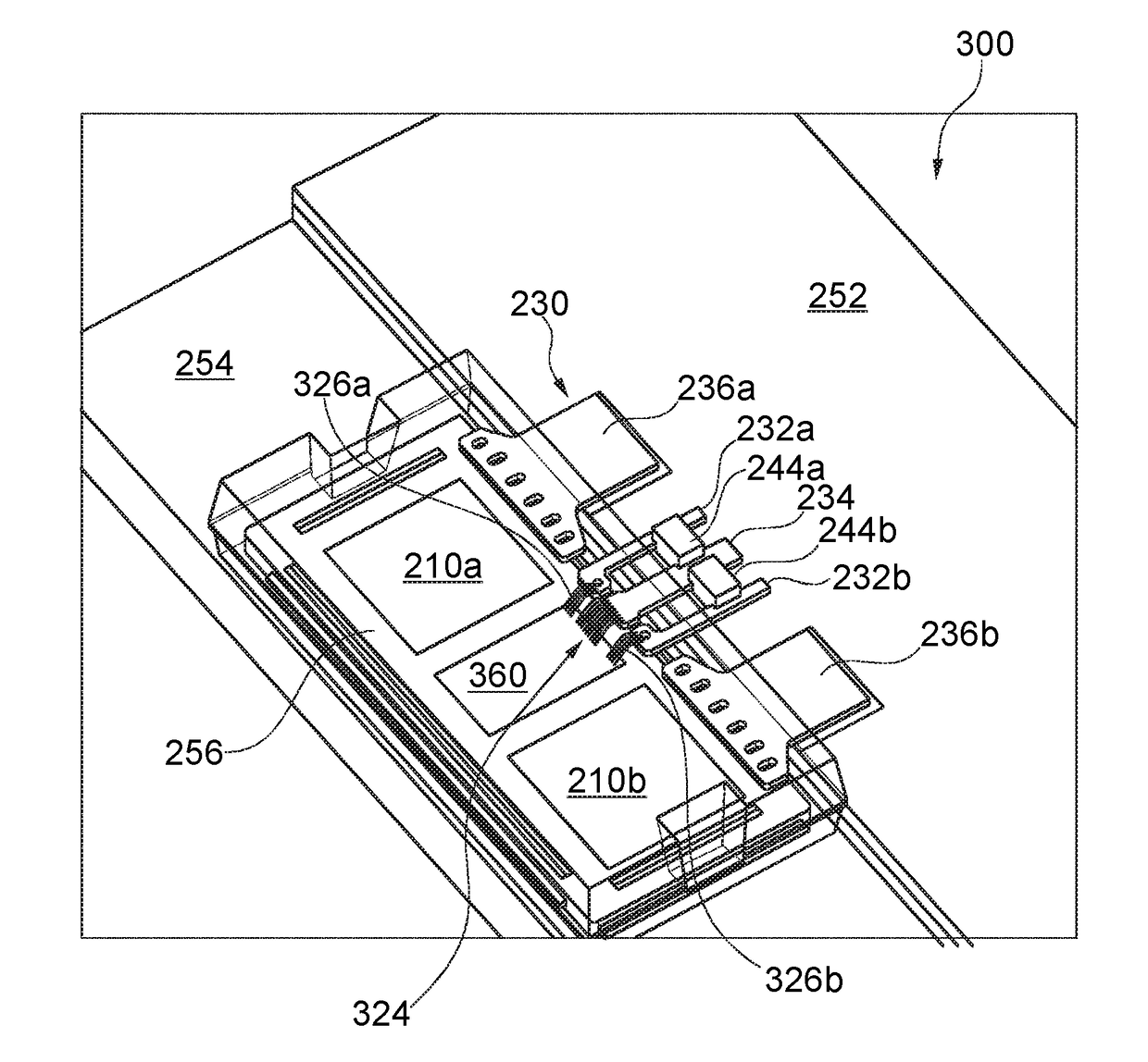
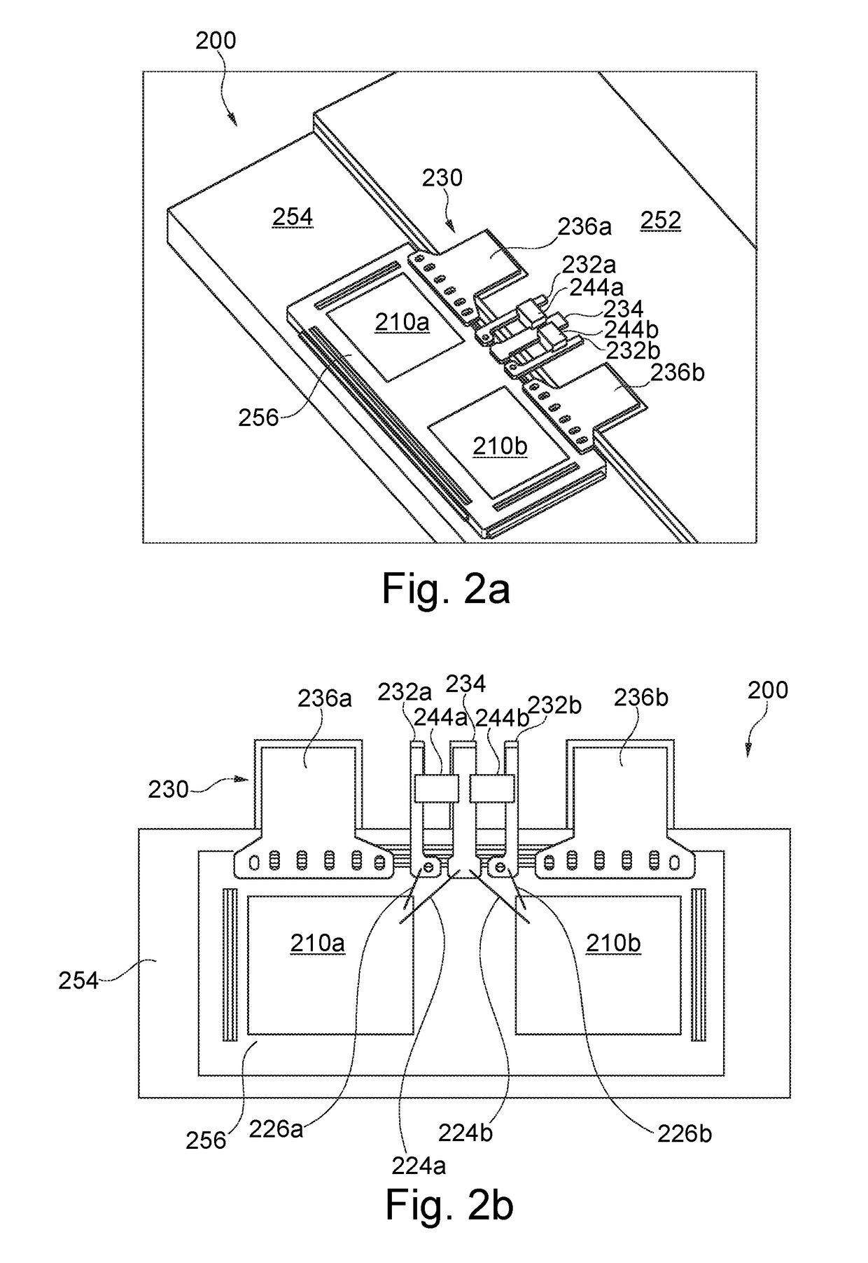
[0058]The illustration in the drawing is schematically. It is noted that in different figures, similar or identical elements or features are provided with the same reference signs or with reference signs, which are different from the corresponding reference signs only within the first digit. In order to avoid unnecessary repetitions elements or features which have already been elucidated with respect to a previously described embodiment are not elucidated again at a later position of the description.

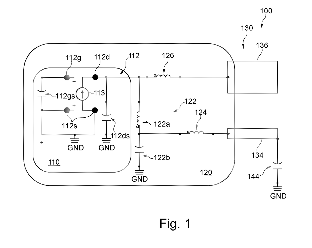
[0059]FIG. 1 shows a circuit diagram of a packaged RF power transistor device 100 in accordance with an embodiment of the invention. The packaged RF power transistor device 100 comprises a die 110 being arranged within a package 120. A lead configuration 130 comprising an RF output lead 136 and a video lead 134 leads through a housing of the package 120 to the outside. It is mentioned that at least one lead, which connects the packaged RF power transistor device to ground, is not depicte...


PUM


Abstract

A packaged Radio Frequency power transistor device is described, which comprises a component carrier a die comprising a semiconductor transistor having a source, a gate and a drain, wherein the die is mounted at the component carrier, a ground connection being electrically connected to the source, an output lead being electrically connected to the drain, a resonance circuit being electrically inserted between the output lead and the ground connection, and a video lead being electrically connected to the resonance circuit. The video lead is configured for being connected to a first contact of a decoupling capacitor. The ground connection is configured for being connected to a second contact of the decoupling capacitor. It is further described a RF power amplifier comprising such a packaged Radio Frequency power transistor device.

Description

CROSS-REFERENCE TO RELATED APPLICATIONS[0001]This application claims the priority under 35 U.S.C. §119 of European patent application no. 13195160.0, filed on Nov. 29, 2014, the contents of which are incorporated by reference herein.FIELD OF THE INVENTION[0002]The present invention relates to the technical field of semiconductor devices being used in power amplifiers. In particular, the present invention relates to a packaged Radio Frequency power transistor device having a certain lead configuration and to a Radio Frequency power amplifier comprising such a packaged Radio Frequency power transistor device.BACKGROUND OF THE INVENTION[0003]Radio Frequency (RF) power amplifiers (PA) are widely used in particular in wireless communication applications such as e.g. cellular network radio base station amplifiers. With the recent growth in the demand for wireless services, the operating frequency for wireless networks and, as a consequence also for RF PA, has increased dramatically and is...

Claims


Application Information

Patent Timeline
Patent Type & Authority Patents(United States)
IPC IPC(8): H05K7/14H03F3/24H03F3/189H03F1/56H01L23/66
CPCH03F1/56H05K7/14H01L23/66H03F3/189H03F3/245H03F2200/387H01L2924/0002H03F2200/222H01L2223/665H01L2223/6644H01L2924/00H01L24/49H01L2924/19107H01L2224/49175H01L2224/49173H01L2924/1421H01L2224/49113H01L2224/49109H01L2224/48195H01L2924/19105H01L2224/48247H01L2224/32245H01L2224/73265H01L24/48H01L2924/00012
Inventor ZHU, YIVAN DER ZANDEN, JOSEPHUS
Owner AMPLEON NETHERLANDS
Why Eureka
Try Eureka