Smart cards having thin die

a technology of thin dies and smart cards, applied in the field of thin dies, can solve the problems of inability to use semiconductor dies of about 0.030 inches thick, failure of existing smart cards, and inability to meet the requirements of rf, so as to improve mechanical flexural resistance and enhance performan

Inactive Publication Date: 2002-04-09
LUCENT TECH INC
View PDF9 Cites 69 Cited by
  • Summary
  • Abstract
  • Description
  • Claims
  • Application Information

AI Technical Summary

Benefits of technology

Improved smart card semiconductor die are provided that have a thickness of approximately 0.004 to 0.007 inches. These die are positioned at or near the neutral plane (i.e., plane of substa

Problems solved by technology

Existing smart cards may fail when, due to applied mechanical stress, the semiconductor die of the smart card breaks.
To this end, note that it is not feasible to use semiconductor die that are about 0.030 inches thick.
Semiconductor die thinner than 0.011 inches are typically not used in smart cards, as such die have traditionally been difficult to handle during the manufacturing process, and the resulting manufacturing expenses are relatively high.
Furthermore, conventional wisdom dictates that, as the thickness of a die is decreased, the die become increasingly vulnerable to mechanical failure.
A shortcoming of existing 0.011-inch die is that the die do not provide sufficient immunity to mechanical flexure.
When such die are used to fabricate smart cards, breakage and card failure may result if the smart card user bends or flexes the card.
Another shortcoming of existing smart card semiconductor die designs is that little, if any, consideration is given to RF (radio frequency) performance issues.
Although transponder devices and pagers have been developed for use at higher frequencies, such devices occupy a much larger physical volume than is available within the confines of a smart card.
That same lead, used at 500 Mhz, provides an inductive reactance of several hundred ohms, which may severely disrupt desired circuit operations at higher frequencies.
Moreover, when an existing semiconductor dice having a thickness of 0.011 inches is u

Method used


Image

  • Smart cards having thin die
  • Smart cards having thin die
  • Smart cards having thin die

Examples


first embodiment

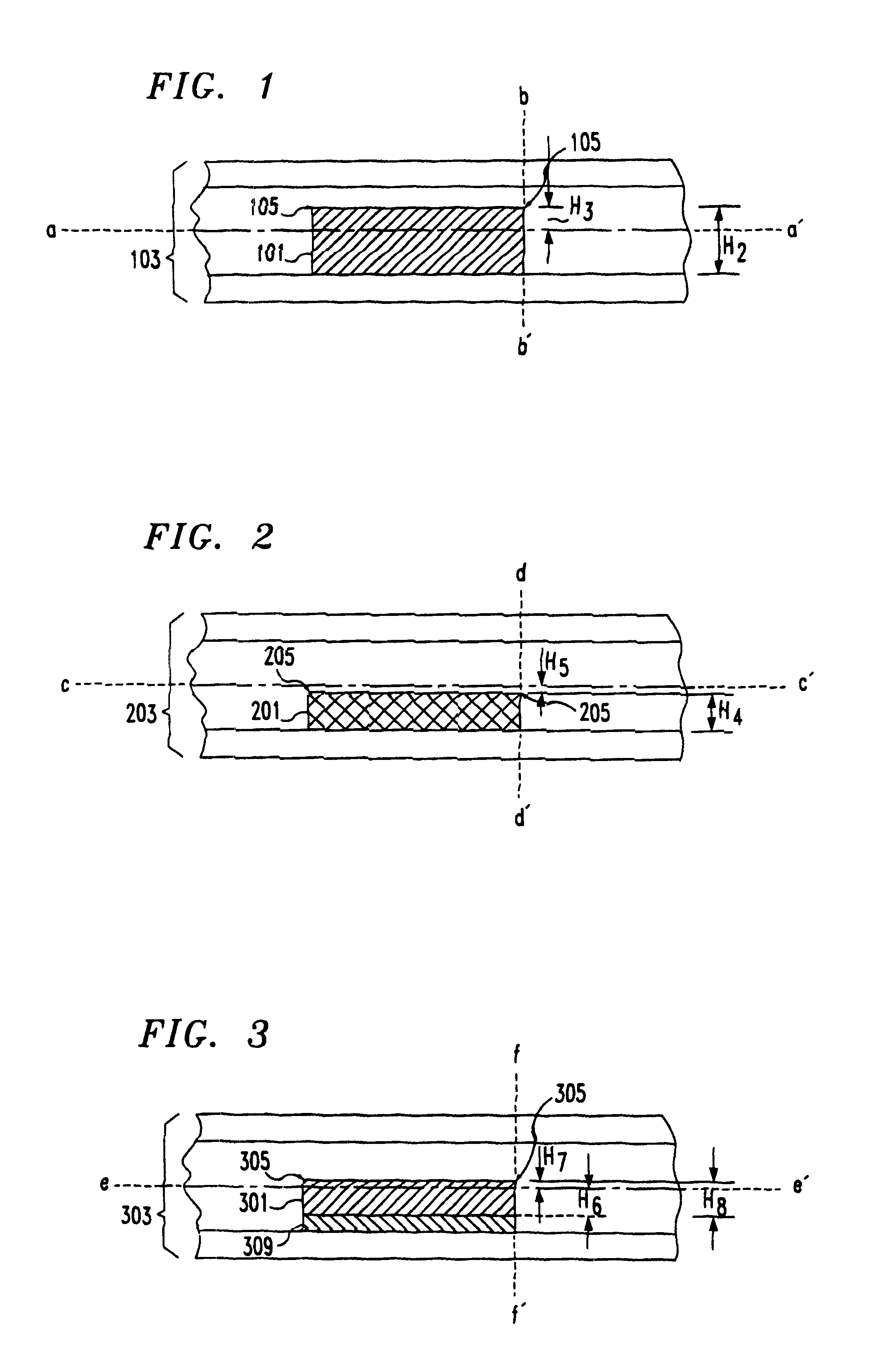
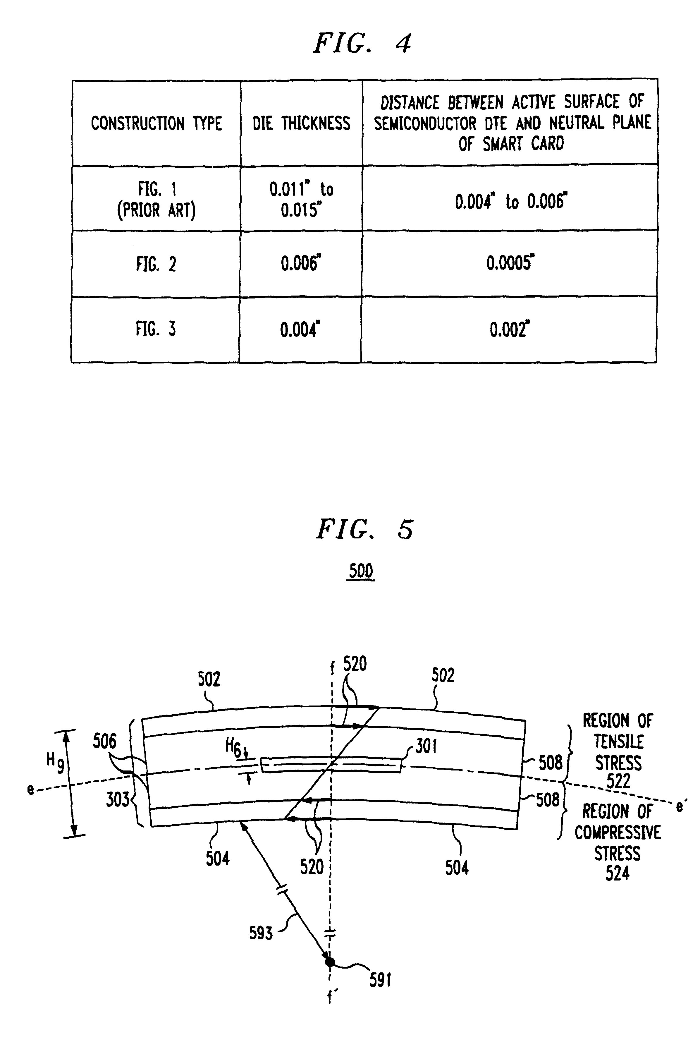
FIG. 2 is a cross-sectional view of a smart card semiconductor die 201 fabricated in accordance with a first embodiment disclosed herein. Typically active devices, such as transistors and diodes, are fabricated near active surface 205 of semiconductor die 201. Smart card package 203 has a neutral plane which, in the cross sectional view of FIG. 2, is represented by axis c-c'. However, unlike the semiconductor die 101 of FIG. 1, semiconductor die 201 has a thickness along axis d-d' of about 0.004 inches, represented as H.sub.4. Axis d-d' may be conceptualized as running parallel to the thinnest dimension of semiconductor 201, and / or running perpendicular to a plane including semiconductor die 201. The semiconductor die active surface 205 is situated at a distance H.sub.5 of 0.001 inches or less from the smart card neutral plane, represented as axis c-c' in FIG. 2.

Although the semiconductor die 201 of FIG. 2 is very thin compared to typical 0.011-inch die, the use of a thin die is adv...

second embodiment

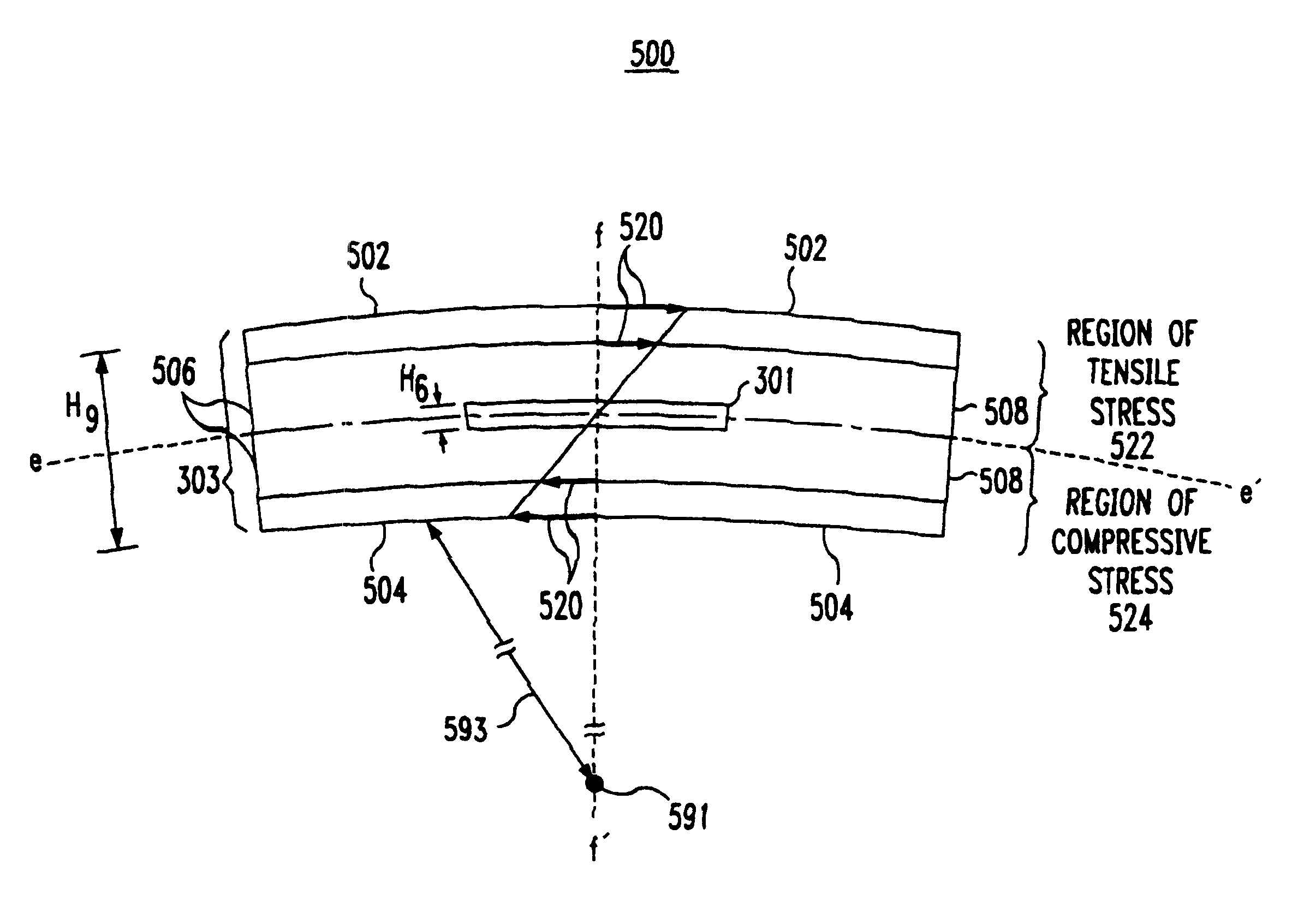
FIG. 3 is a cross-sectional view of a thin smart card semiconductor die 301 fabricated in accordance with a second embodiment disclosed herein. As in the case of semiconductor die 201 of FIG. 2, active devices, such as transistors and diodes, are fabricated near active surface 305 of semiconductor die 301. Smart card package 303 has a neutral plane which, in the cross sectional view of FIG. 3, is represented by axis e-e'. Unlike the semiconductor die 101 of FIG. 1, semiconductor die 301 has a thickness along axis f-f' of about 0.004 inches, represented as H.sub.8. The semiconductor die active surface 305 is situated at a distance H.sub.7 of 0.001 inches or less from the smart card neutral plane, represented as axis e-e' in FIG. 3. Unlike the semiconductor die 201 of FIG. 2, semiconductor 301 is mounted to smart card package 303 using a physical standoff 309. Physical standoff 309 functions as a mechanical spacer, holding the active semiconductor die 301 at a desired spatial relation...


PUM


Abstract

Thin semiconductor die, approximately 0.004 to 0.007 inches thick, are positioned substantially on the neutral plane of a smart card, the neutral plane defined as the plane of substantially no mechanical strain during flexure of the smart card, thereby providing smart cards having improved resistance to mechanical flexure, and/or smart cards having improved RF performance.

Description

CROSS-REFERENCE TO RELATED APPLICATIONRelated subject matter is disclosed in the co-pending, commonly assigned U.S. patent application of E. Suhir--1, Ser. No. 08 / 551,241, filed on Oct. 31, 1995, entitled "Data Carriers Having An Integrated Circuit Unit", in the co-pending, commonly-assigned U.S. patent application of Clifton-Flynn-Verdi 4-6-15, Ser. No. 08 / 558,579, filed on Oct. 31, 1995, entitled, "Smart Card Having a Thin Die", and in U.S. Pat. No. 5,480,842 issued on Jan. 2, 1996 to Clifton, Flynn, and Verdi.BACKGROUND OF THE INVENTION1. Field of the InventionThis invention relates generally to semiconductor devices, and more particularly to semiconductor die that are used in the manufacture of smart cards.2. Background ArtExisting smart cards may fail when, due to applied mechanical stress, the semiconductor die of the smart card breaks. Mechanical stress is inherent in typical smart card operational environments, such as point-of-sale terminals, electronic cash machines, credi...

Claims


Application Information

Patent Timeline
IPC IPC(8): G06K19/077H01L23/04H01L23/08
CPCG06K19/07728G06K19/07745H01L2924/0002H01L2924/00
Inventor CLIFTON, MARK BRADFORDFLYNN, RICHARD MICHAELVERDI, FRED WILLIAM
Owner LUCENT TECH INC
Why Eureka
Try Eureka