
Laser segmented cutting, multi-step cutting, or both

a laser cutting and segmented technology, applied in welding/soldering/cutting articles, manufacturing tools, electric/magnetic/electromagnetic heating, etc., can solve the problems of increasing chipping, curved or slanting cuts, and dicing blades tend to wear relatively quickly, so as to improve the throughput of laser cutting silicon or other materials

Inactive Publication Date: 2012-08-28
ELECTRO SCI IND INC
View PDF132 Cites 22 Cited by
  • Summary
  • Abstract
  • Description
  • Claims
  • Application Information

AI Technical Summary

Benefits of technology

[0012]An object of the present invention is, therefore, to provide a method and / or system for improving the throughput for laser cutting silicon or other materials.
[0013]As a result, laser sawing is becoming an attractive alternative to these conventional techniques for dicing. Some reasons for the consideration of laser dicing would be that lasers can cut curved die such as Arrayed Waveguide Gratings (AWGs) from a wafer, unlike either of the two conventional techniques. In addition, lasers can often cut without the use of water, which is of great importance for the manufacture of devices which are water sensitive, such as MEMS. Dicing saws, which are today the predominant technique in use, typically require the use of water as a lubricant and / or coolant. Lasers also offer the potential of the smallest street width available, due to a potentially very small kerf width and the possibility of very accurate alignment of the laser to the workpiece (wafer).

Problems solved by technology

Skilled persons will also note that dicing blades tend to wear relatively quickly such that the widths of their cuts may vary over time.
In some cases, the blades can be inadvertently bent and then such blades produce curved or slanted cuts or increased chipping.
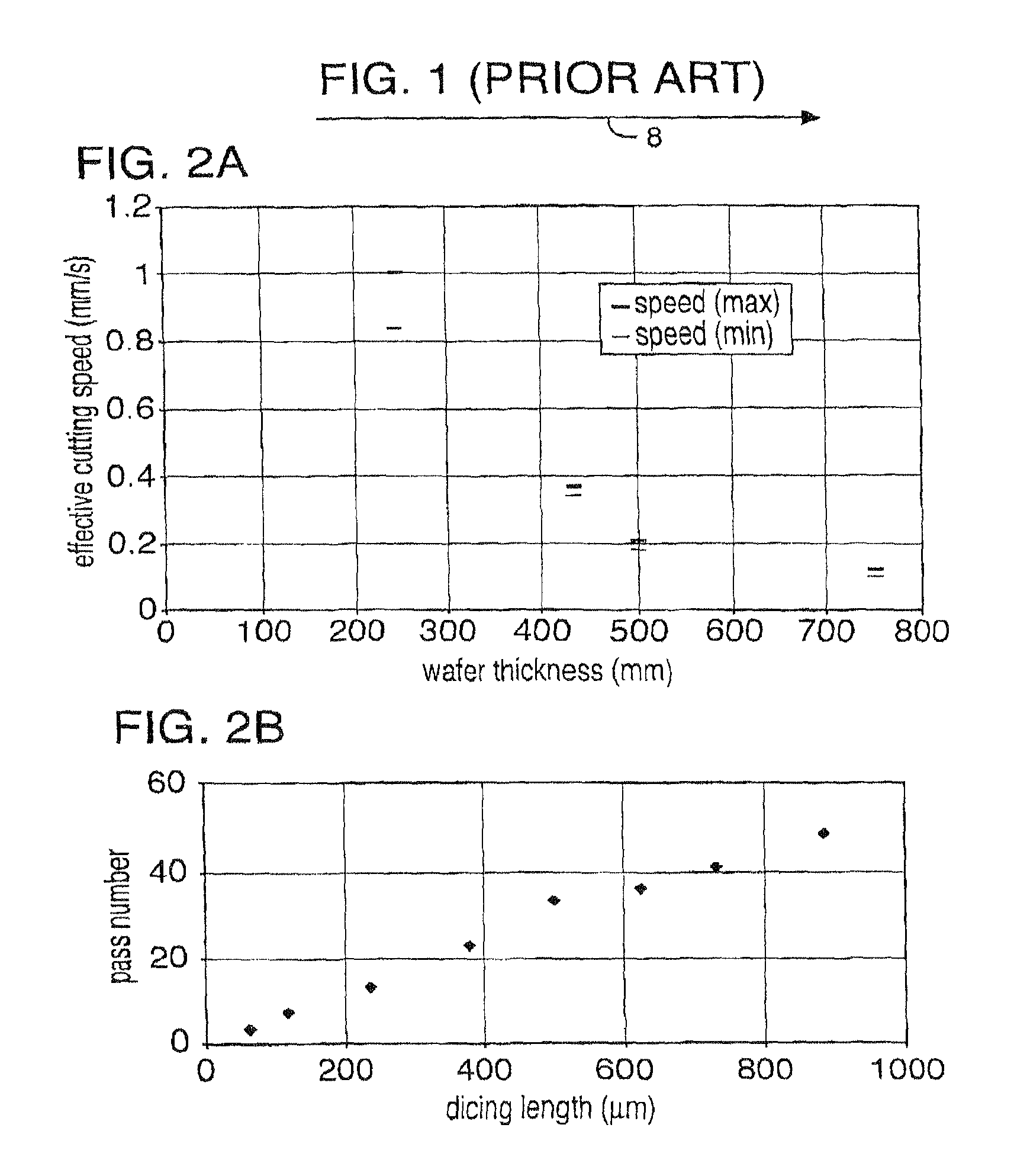
When the target material is thick, many passes (in some cases over 100 passes) may be necessary to complete the cutting process, particularly with limited laser power.

Method used


Image

  • Laser segmented cutting, multi-step cutting, or both
  • Laser segmented cutting, multi-step cutting, or both
  • Laser segmented cutting, multi-step cutting, or both

Examples


Embodiment Construction

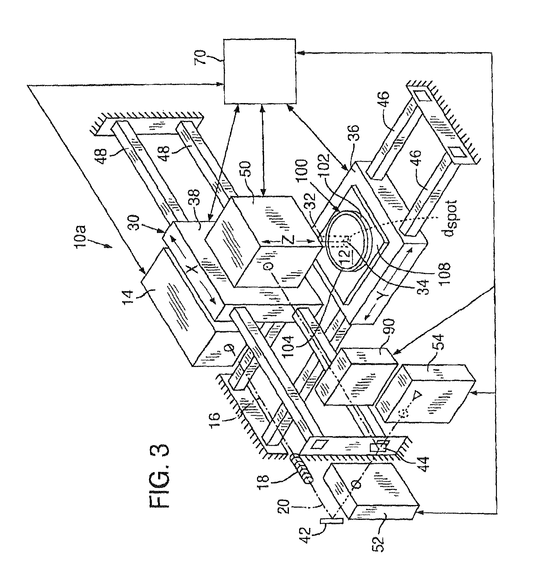
[0086]FIGS. 3 and 4 illustrate alternative embodiments of respective exemplary laser processing systems 10a and 10b (generically 10) utilizing a compound beam positioning system 30 equipped with a wafer chuck assembly 100 that can be employed for performing segmented cutting, such as trenching, slicing, or dicing semiconductor workpieces 12, in accordance with the present invention. With reference to FIGS. 3 and 4, an exemplary embodiment of a laser system 10 includes a Q-switched, diode-pumped (DP), solid-state (SS) UV laser 14 that preferably includes a solid-state lasant such as Nd:YAG, Nd:YLF, Nd:YAP, or Nd:YVO4, or a YAG crystal doped with holmium or erbium. Laser 14 preferably provides harmonically generated UV laser output 16 of one or more laser pulses at a wavelength such as 355 nm (frequency tripled Nd:YAG), 266 nm (frequency quadrupled Nd:YAG), or 213 nm (frequency quintupled Nd:YAG) with primarily a TEM00 spatial mode profile.

[0087]In a preferred embodiment, laser 14 inc...


PUM

PropertyMeasurementUnit
dimensionaaaaaaaaaa
diameteraaaaaaaaaa
diameteraaaaaaaaaa

Abstract

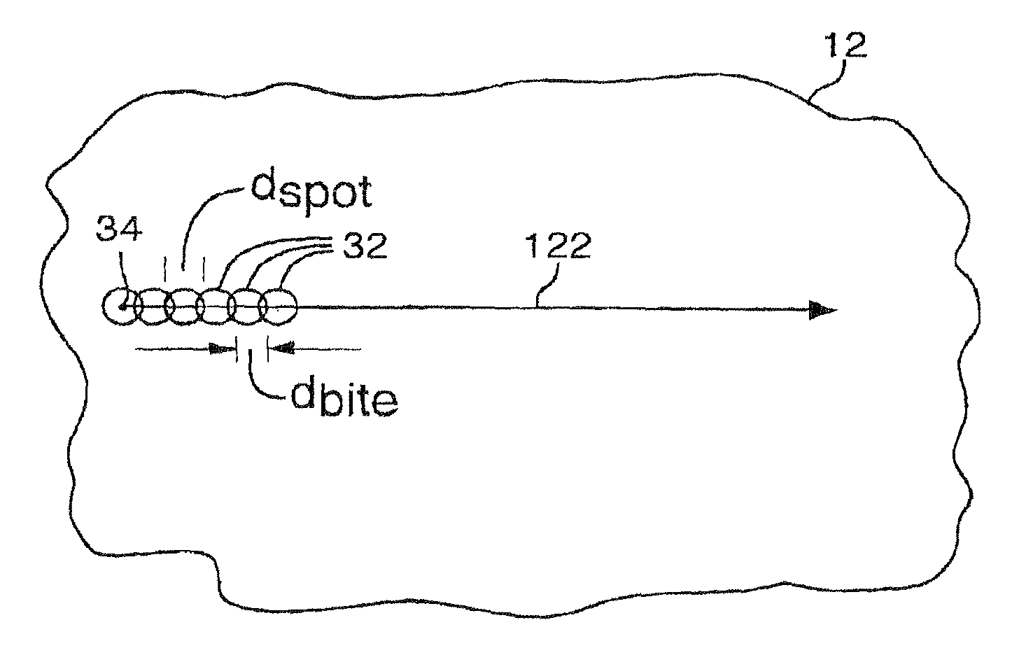
UV laser cutting throughput through silicon and like materials is improved by dividing a long cut path (112) into short segments (122), from about 10 μm to 1 mm. The laser output (32) is scanned within a first short segment (122) for a predetermined number of passes before being moved to and scanned within a second short segment (122) for a predetermined number of passes. The bite size, segment size (126), and segment overlap (136) can be manipulated to minimize the amount and type of trench backfill. Real-time monitoring is employed to reduce rescanning portions of the cut path 112(112) where the cut is already completed. Polarization direction of the laser output (32) is also correlated with the cutting direction to further enhance throughput. This technique can be employed to cut a variety of materials with a variety of different lasers and wavelengths. A multi-step process can optimize the laser processes for each individual layer.

Description

NOTICE[0001]More than one application for reissue of U.S. Pat. No. 6,676,878 has been filed. The reissue applications are U.S. patent application Ser. Nos. 12 / 351,562, (the present application), 12 / 350,767, 12 / 256,156, and 11 / 332,815, all of which are divisional applications for reissue of U.S. Pat. No. 6,676,878.RELATED APPLICATIONS[0002]This is an application for reissue of U.S. Pat. No. 6,676,878 and a division of U.S. patent application Ser. No. 11 / 332,815 filed Jan. 13, 2006, which is an application for reissue of U.S. Pat. No. 6,676,878.[0003]This patent applicationU.S. patent application Ser. No. 10 / 165,428, filed Jun. 6, 2002, on which U.S. Pat. No. 6,676,878 issued, derives priority from U.S. Provisional Application No. 60 / 297,218, filed Jun. 8, 2001, and is a CIP of U.S. patent application Ser. No. 10 / 017,497, filed Dec. 14, 2001, (now U.S. Pat. No. 7,157,038), which claims priority from U.S. Provisional Application No. 60 / 265,556, filed Jan. 31, 2001, and is a CIP of U.S....

Claims


Application Information

Patent Timeline
Patent Type & Authority Patents(United States)
IPC IPC(8): B23K26/04C04B41/91B23K26/03B23K26/073B23K26/14B23K26/38B23K26/40
CPCB23K26/032B23K26/073B23K26/083B23K26/0869B23K26/38B23K26/40B23K26/0622B23K26/066B23K26/364B23K2101/40B23K2103/50
Inventor O'BRIEN, JAMES N.ZOU, LIAN-CHENGSUN, YUNLONGFAHEY, KEVIN P.WOLFE, MICHAEL J.BAIRD, BRIAN W.HARRIS, RICHARD S.
Owner ELECTRO SCI IND INC
Learn More