
Ferroelectric film capacity used for ferroelectric memorizer and its manufacturing method
A technology of ferroelectric memory and ferroelectric thin film, which is applied in the fields of electric solid device, semiconductor/solid state device manufacturing, circuit, etc. Large polarization, good fatigue characteristics, good compatibility
- Summary
- Abstract
- Description
- Claims
- Application Information
AI Technical Summary
Problems solved by technology
Method used
Image

Examples
Embodiment 1
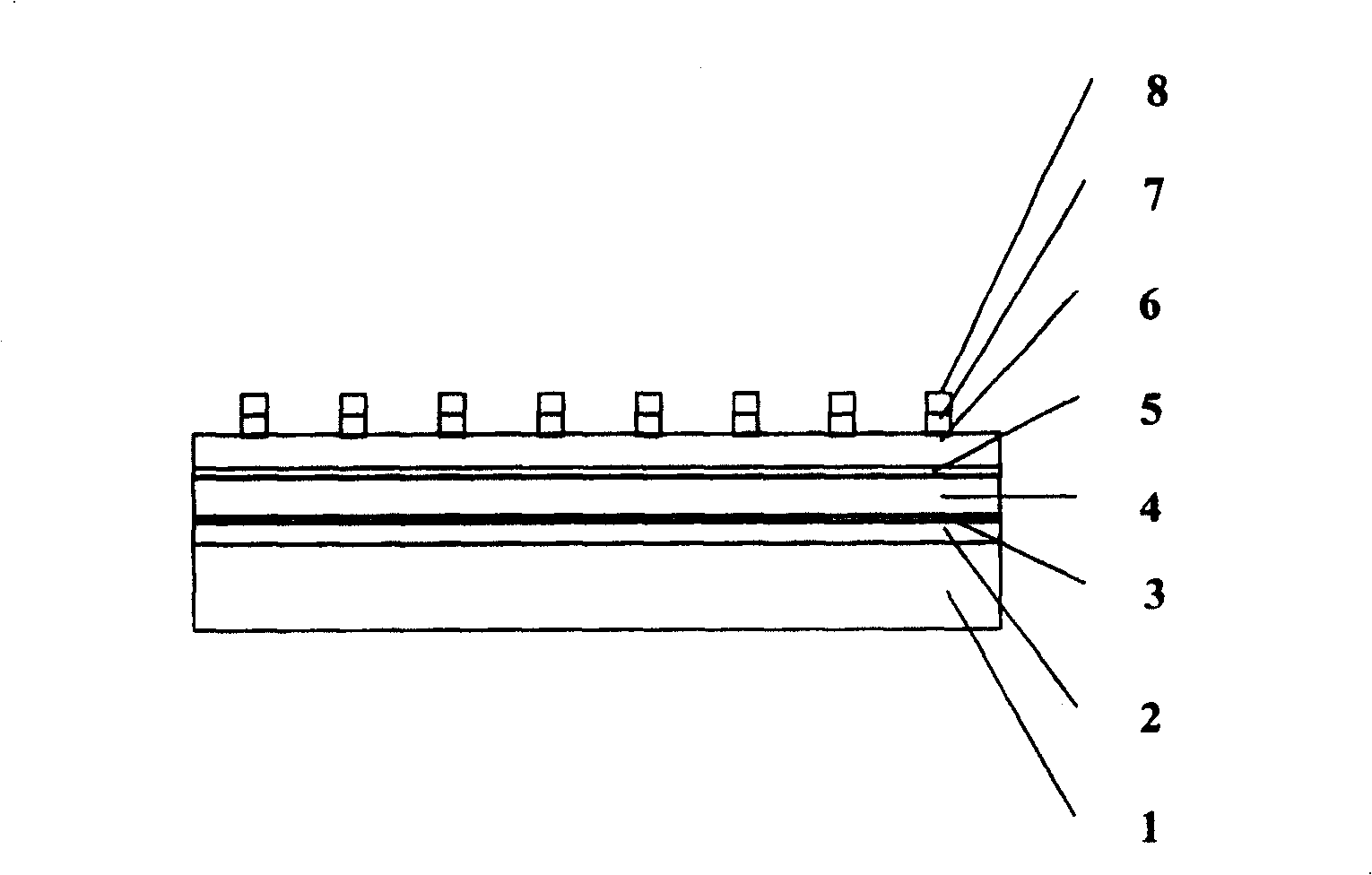
[0031] Embodiment 1 A method for preparing a ferroelectric film capacitor for ferroelectric memory, including
[0032] ① Surface treatment and cleaning of silicon substrate 1 according to standard CMOS process;
[0033] ② Using the thermal oxidation method, a 150nm thick silicon dioxide barrier layer 2 is formed on the surface of the silicon substrate 1;
[0034] ③Use magnetron sputtering method to prepare 20nm thick titanium dioxide bonding layer 3 on the silicon dioxide barrier layer 2. The magnetron sputtering process conditions are: sputtering pressure 1.5Pa, sputtering substrate temperature 200℃, sputtering Shooting atmosphere is O 2 :Ar=1:9;
[0035] ④Prepare 150nm thick bottom electrode metal layer Pt4 on the titanium dioxide bonding layer 3 by magnetron sputtering. The process conditions of magnetron sputtering are: sputtering pressure 1Pa, sputtering substrate temperature 200℃, sputtering atmosphere Is Ar gas;
[0036] ⑤ LSMO target material is prepared by standard solid ...
Embodiment 2
[0047] Embodiment 2 A method for preparing a ferroelectric film capacitor for ferroelectric memory, including
[0048] ① Surface treatment and cleaning of silicon substrate 1 according to standard CMOS process;
[0049] ② Using thermal oxidation method, a 120nm thick silicon dioxide barrier layer 2 is formed on the surface of the silicon substrate 1;
[0050] ③ Use magnetron sputtering method to prepare 30nm thick titania bonding layer 3 on the silicon dioxide barrier layer 2. The magnetron sputtering process conditions are: sputtering pressure 0.5Pa, sputtering substrate temperature 300℃, sputtering Shooting atmosphere is O 2 :Ar=2:9;
[0051] ④A 150nm thick lower electrode metal layer Pt4 is prepared on the titanium dioxide bonding layer 3 by magnetron sputtering. The magnetron sputtering process conditions are: sputtering pressure 0.5Pa, sputtering substrate temperature 300℃, sputtering The atmosphere is Ar gas;
[0052] ⑤Prepare the LSMO target by standard solid-phase reaction...
Embodiment 3
[0059] Embodiment 3 A method for preparing a ferroelectric film capacitor for ferroelectric memory, including
[0060] ① Surface treatment and cleaning of silicon substrate 1 according to standard CMOS process;
[0061] ②Using thermal oxidation method to generate 200nm thick silicon dioxide barrier layer 2 on the surface of silicon substrate 1;
[0062] ③Use magnetron sputtering method to prepare 20nm thick titania bonding layer 3 on the silicon dioxide barrier layer 2. The magnetron sputtering process conditions are: sputtering pressure 1Pa, sputtering substrate temperature 200℃, sputtering The atmosphere is O 2 :Ar=1:9;
[0063] ④ Use magnetron sputtering method to prepare 100nm thick bottom electrode metal layer Pt4 on the titanium dioxide bonding layer 3. The process conditions of magnetron sputtering are: sputtering pressure 1Pa, sputtering substrate temperature 200℃, sputtering atmosphere Is Ar gas;
[0064] ⑤Prepare the LSMO target by standard solid-phase reaction method, a...
PUM
| Property | Measurement | Unit |
|---|---|---|
| thickness | aaaaa | aaaaa |
| thickness | aaaaa | aaaaa |
| thickness | aaaaa | aaaaa |
Abstract
Description
Claims
Application Information