Electrode of gallium nitride base III-V. class compound semiconductor
A gallium nitride-based and compound technology is applied in semiconductor devices, semiconductor/solid-state device parts, electric solid-state devices, etc. It can solve the problems of not being able to make two electrodes at the same time, increasing the forward voltage drop Vf of the device, and device leakage current Ir increase and other issues, to achieve good reflective properties, enhanced reliability, and simple manufacturing process
- Summary
- Abstract
- Description
- Claims
- Application Information
AI Technical Summary
Problems solved by technology
Method used
Image
Examples
Embodiment 1
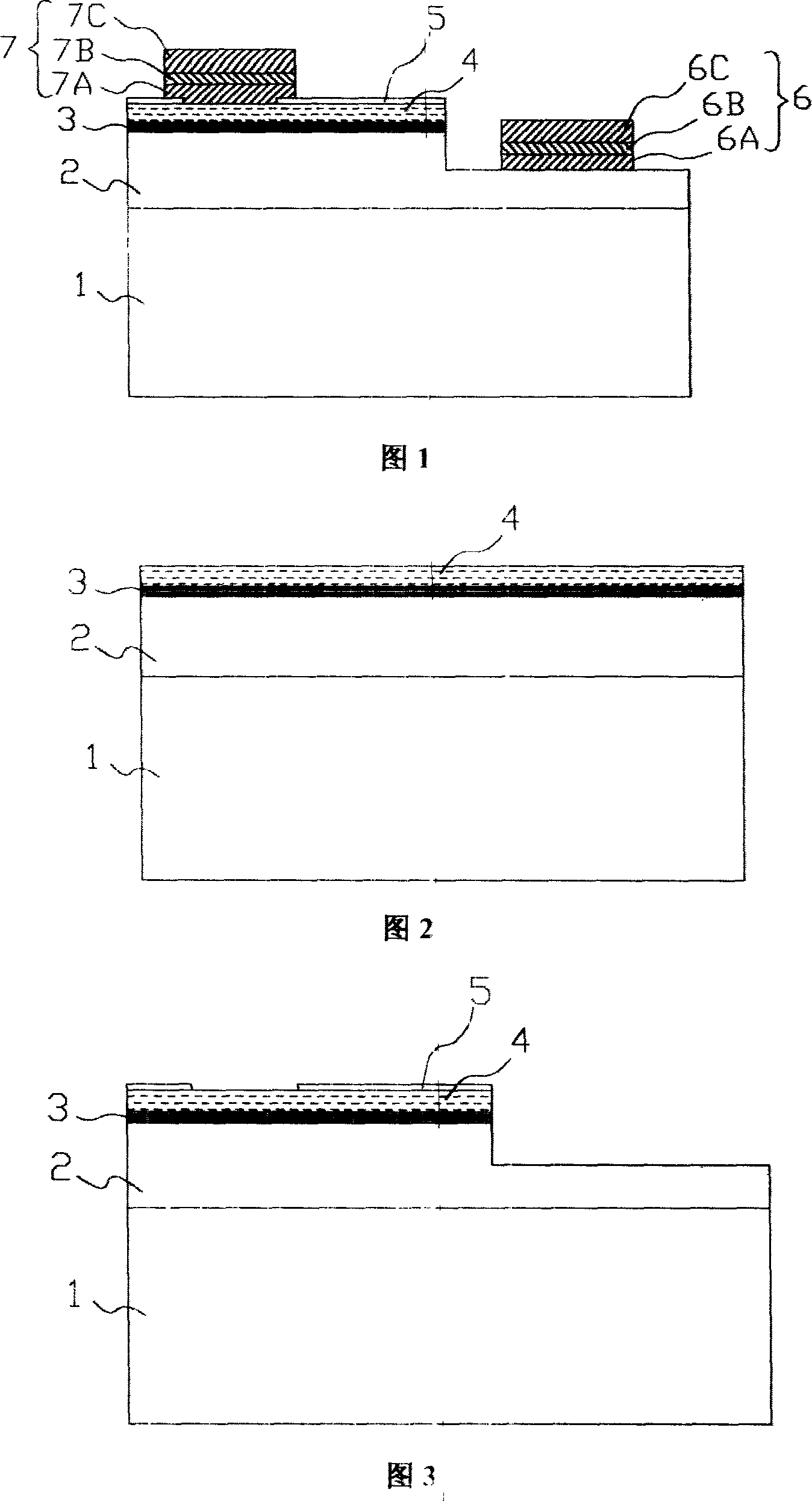
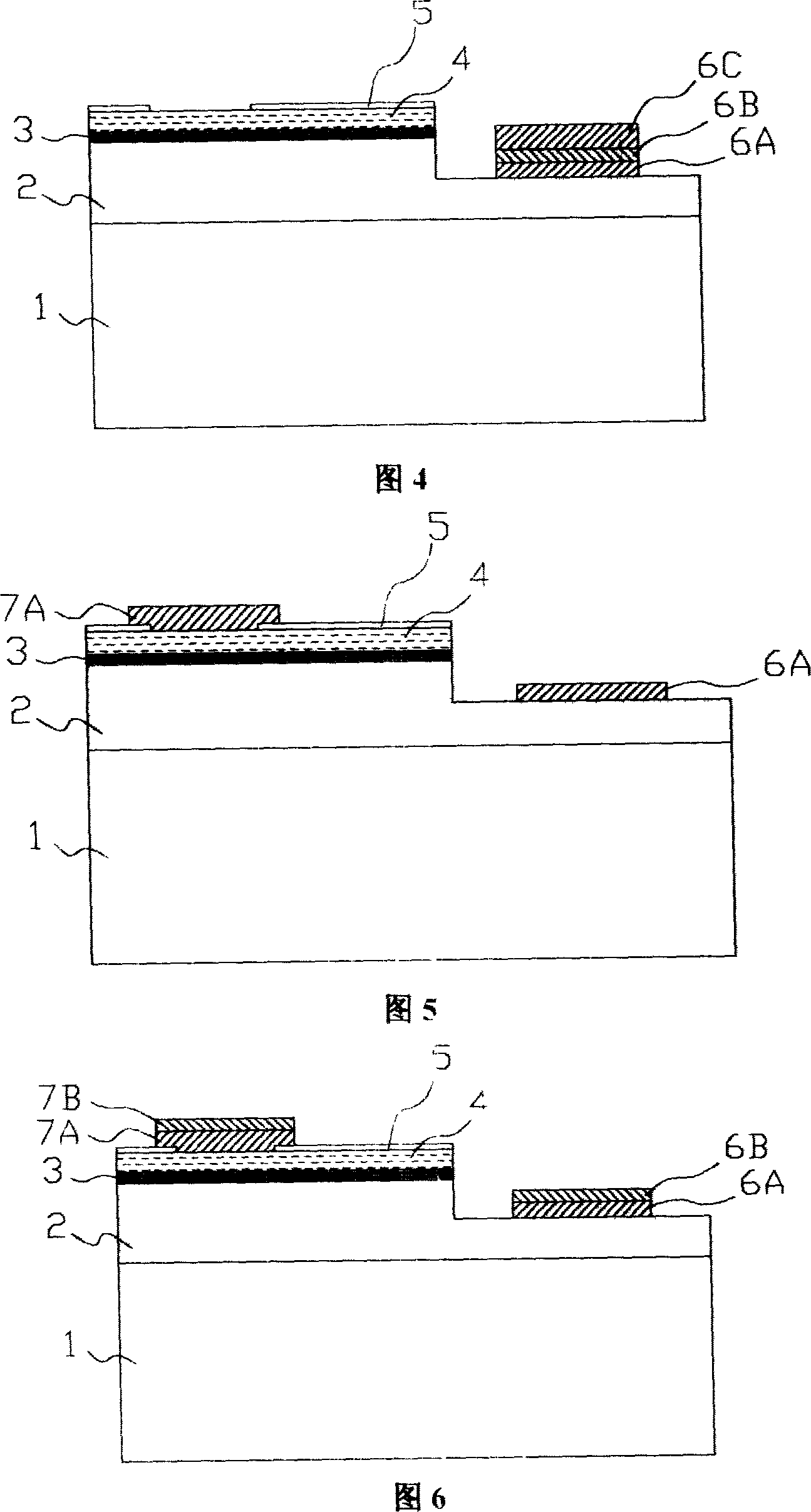
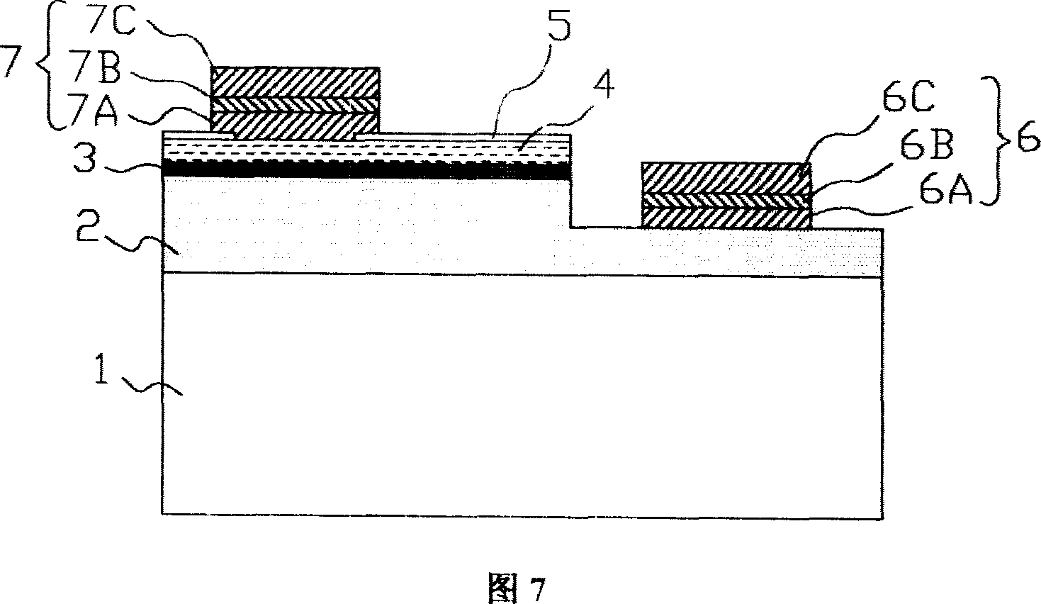
[0033] See Figures 2, 3, 4 and 7. First, the sapphire epitaxial wafer as shown in Figure 2 is etched with reactive ion etching to remove part of the p-GaN layer 4, the multilayer quantum well layer 3, and the n-GaN layer 2, so that an n- GaN platform. Then a layer of transparent electrode 5 is evaporated on the p-GaN region, and it is heat-treated to form an ohmic contact with the p-GaN layer 4 (as shown in FIG. 3 ). Then, Cr / Pt / Al is evaporated sequentially on the etched n-GaN platform, and then the metal lift-off process is used to form an ohmic contact layer 6A, a metal barrier layer 6B and a bonding layer 6C in the n-GaN region (as shown in Figure 4 shown). And the n electrode is annealed to make it form a good ohmic contact with the n-GaN region. Then, Cr / Pt / Al is sequentially evaporated on the p-GaN region, and a metal lift-off process is used to form an adhesive conductive layer 7A, a metal barrier layer 7B and a bonding layer 7C in the p-GaN region (as shown in FIG....
Embodiment 2
[0035]See Figures 2, 3, 5, 6 and 7. As in Embodiment 1, an n-GaN platform is etched on the sapphire epitaxial wafer, and a layer of transparent electrode 5 is evaporated to form an ohmic contact. Then sequentially evaporate Cr / Pt / Al on the n-GaN region and the p-GaN region, and then use the metal lift-off process to form the ohmic contact layer 6A and the adhesive conductive layer 7A of the n-GaN region and the p-GaN region, Metal barrier layers 6B, 7B and bonding layers 6C, 7C (as shown in FIG. 5 , FIG. 6 , and FIG. 7 ).
PUM
 Abstract
Description
Claims
Application Information


