Hemi-spherical shape and spherical two-photon response semiconductor photoelectric detector

A photodetector and semiconductor technology, applied in the field of information science and technology, can solve problems such as complex manufacturing process

Inactive Publication Date: 2007-08-08
JILIN UNIV
View PDF0 Cites 7 Cited by
  • Summary
  • Abstract
  • Description
  • Claims
  • Application Information

AI Technical Summary

Problems solved by technology

However, the manufacturing process of such devices is complex

Method used


Image

  • Hemi-spherical shape and spherical two-photon response semiconductor photoelectric detector

Examples


Embodiment 1

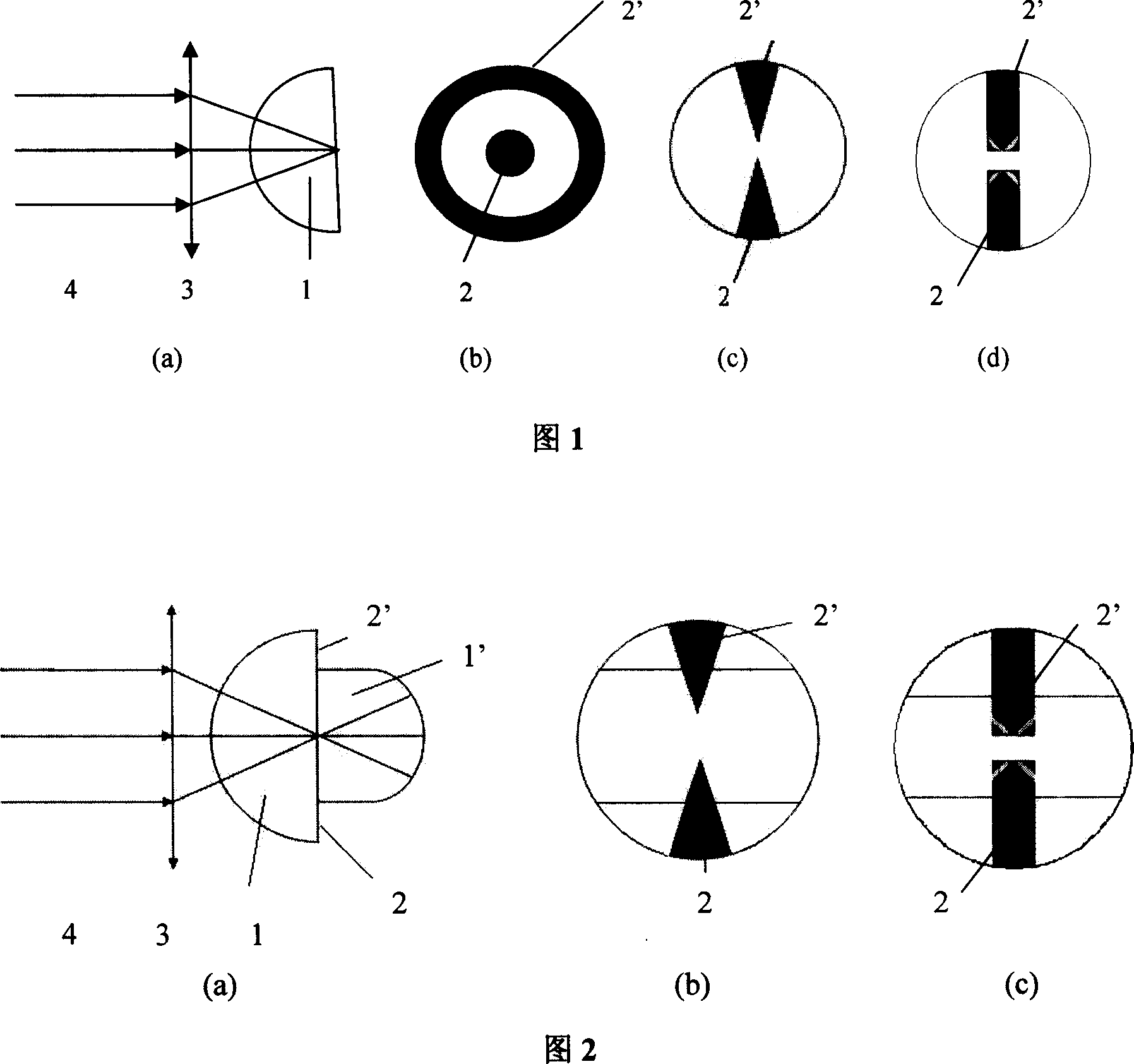
[0031] 1. The wavelength of the laser to be measured is 1.3 microns, the photon energy is 0.95 electron volts, and the photon energy of the frequency-doubled light is 0.95×2=1.8 electron volts. Because GaAs has a forbidden band width of 1.42 electron volts and a refractive index of about 3.4, a semi-insulating GaAs material is selected to make a hemispherical two-photon response photodetector.

[0032] 2. Select a microscope objective lens with a numerical aperture (NA) of 0.3 and a working distance of 6 mm for focusing. The radius of the GaAs hemisphere was determined to be 3 mm.

[0033] 3. Using the usual optical lens processing technology, the gallium arsenide material is processed into a hemisphere with a radius of 3 mm. And the usual optical polishing of spherical and flat surfaces. The error is ±0.01 mm, and the finish is grade 2.

[0034] 4. Fabricate metal electrodes in the plane of the hemisphere using conventional semiconductor technology. The aluminum electrode...

Embodiment 2

[0038] 1. The wavelength of the laser to be measured is 1.06 microns, the photon energy is 1.17 eV, and the photon energy of the frequency-doubled light is 1.17×2=2.34 eV. Because the forbidden band width of zinc telluride is 2.26 electron volts, and the refractive index is about 2.7, the unintentionally doped zinc telluride material is selected to make a hemispherical two-photon response photodetector.

[0039] 2. Select a microscope objective lens with a numerical aperture (NA) of 0.3 and a working distance of 6 mm for focusing. The radius of the ZnTe hemisphere was determined to be 3 mm.

[0040] 3. Using optical lens processing technology, the zinc telluride material is processed into a hemisphere with a radius of 3 mm. And for spherical and flat polishing. The error is ±0.01 mm, and the finish is grade 2.

[0041] 4. Fabricate metal electrodes in the plane of the hemisphere using conventional semiconductor technology. Gold electrodes are deposited in the plane of the ...

Embodiment 3

[0045] 1. The wavelength of the laser to be measured is 1.55 microns, the photon energy is 0.80 electron volts, and the photon energy of the frequency-doubled light is 0.80×2=1.60 electron volts. Because the forbidden band width of silicon is 1.12 electron volts and the refractive index is about 3.4, the near-intrinsic silicon material is selected to make the two-photon response photodetector.

[0046] 2. Select a microscope objective lens with a numerical aperture (NA) of 0.3 and a working distance of 6 mm for focusing. The radius of the silicon hemisphere was determined to be 3 mm.

[0047] 3. Using optical lens processing technology, the silicon material is processed into a hemisphere with a radius of 3 mm. And for spherical and flat polishing. The error is ±0.01 mm, and the finish is grade 2.

[0048] 4. Fabricate metal electrodes in the plane of the hemisphere using conventional semiconductor technology. Aluminum electrodes were evaporated in the plane of the hemisphe...


PUM


Abstract

The invention relates to the hemispherical and spherical two-photon response semiconductor photodetector for the ultrashort optical pulse measurement system, the optoelectronic integrated system and the optical communication system. The hemispherical two-photon response semiconductor photodetector comprises the semiconductor hemisphere (1), the metal electrode pairs (2, 2') and the micro lens (3), and its features are: the radius of the semiconductor hemisphere (1) is less than the work distance of the micro lens (3), and the sphere center of the semiconductor hemisphere (1) locates in the focus of the micro lens (3), and the metal electrode pairs (2, 2') locates in the plane of the semiconductor hemisphere (1), and the incident parallel light (4) passes the focus of the micro lens (3), incident vertical to the spherical surface of the semiconductor hemisphere (1), and going ahead along the radius direction, and finally the focus of the focused beam falls at the spherical center, and imposing the DC voltage to the metal electrode pairs (2, 2'), by the measurement of the optical current, to achieve a relative measurement of the incident light power.

Description

technical field [0001] The invention belongs to the field of information science and technology, and specifically relates to a hemispherical and spherical two-photon response semiconductor photodetector that can be used in ultrashort optical pulse measurement systems, photoelectric integration systems and optical communication systems. technical background [0002] In the 1990s, some people began to use ordinary photodetectors as two-photon response photodetectors to construct optical autocorrelation systems and measure ultrashort light pulses [Y.Takagi, T.Kobayashi, K.Yoshihara, and S . Imamura, Optics Letters 17, 658 (1992); L. P. Barry, P. G. Bollond, J. M. Dudley, J. D. Harvey, and R. Leonhardt, Electronics Letters, 32, 1922 (1996)]. They used a lens to focus the incident light beam onto a common flat-panel photodetector, and replaced the frequency doubling crystal and photomultiplier tube with a two-photon responsive semiconductor photodetector. In terms of photocurren...

Claims


Application Information

Patent Timeline
Patent Type & Authority Applications(China)
IPC IPC(8): G01J1/42G01J11/00H01L31/08
Inventor 贾刚陈占国刘秀环时宝
Owner JILIN UNIV
Why Eureka
Try Eureka