Semiconductor device and its making method

A manufacturing method, semiconductor technology, applied in semiconductor/solid-state device manufacturing, semiconductor devices, transistors, etc., which can solve the problems of recession, silicide and oxide loss, hot carrier lifetime and negative bias temperature instability, etc. Achieve the effects of adjustable stress size, low dielectric constant, and simplified contact hole etching process

Active Publication Date: 2007-08-29
TAIWAN SEMICON MFG CO LTD
View PDF0 Cites 22 Cited by
  • Summary
  • Abstract
  • Description
  • Claims
  • Application Information

AI Technical Summary

Problems solved by technology

However Si 3 N 4 For high dielectric constant materials, it will generate capacitive coupling noise between adjacent voltage transients (capacitive coupling noise)
Since the contact hole etch stop layer is close to the gate oxide layer and Si 3 N 4 Thin film, so transistor performance, such as hot carrier lifetime and negative bias temperature instability, etc., will be greatly degraded
In addition to the above-mentioned problems arising in the etching process for forming the contact hole, the compressive stress film Si 3 N 4 and tensile stress film Si 3 N 4 Has a different etch rate, so more silicide and oxide losses are generated during the etching process to form the contact hole, causing serious leakage current

Method used


Image

  • Semiconductor device and its making method
  • Semiconductor device and its making method
  • Semiconductor device and its making method

Examples


Embodiment Construction

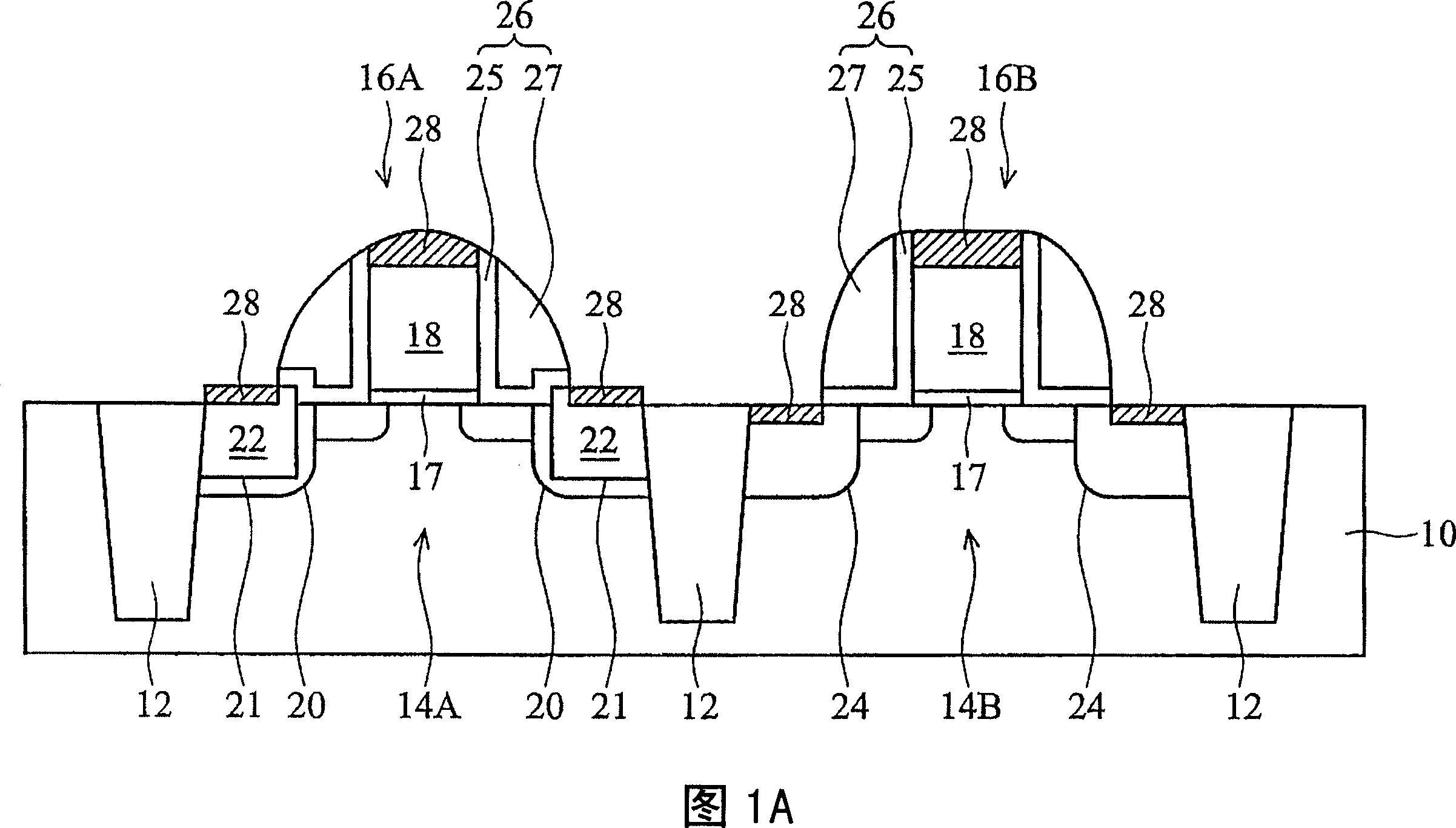
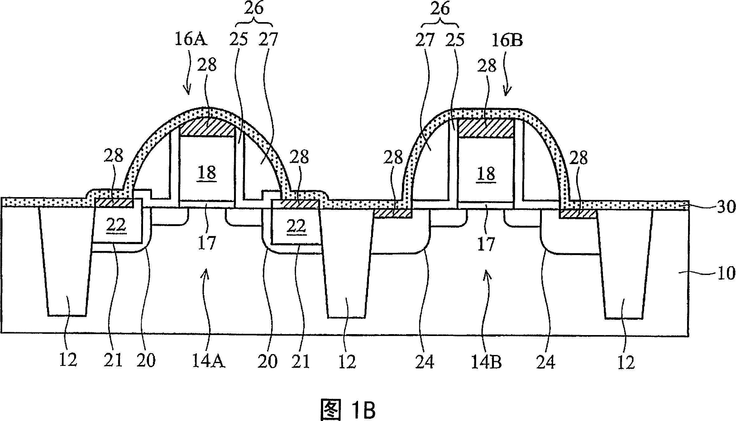
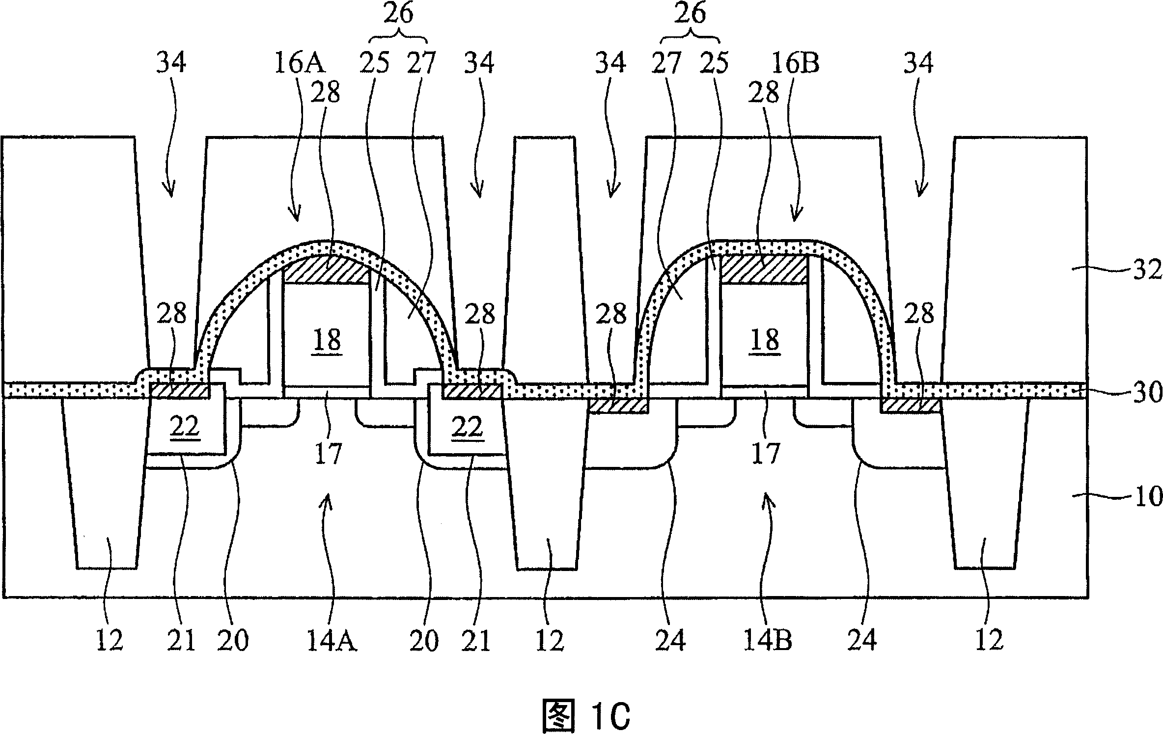
[0043] Embodiments of the present invention provide a strain-enhanced CMOS device and a manufacturing method thereof, in order to use an amorphous carbon film as a stress covering film to solve the problem of using Si in the known technology. 3 N 4 Problems caused by cover film. Amorphous carbon films, such as fluorine-doped amorphous carbon films, are materials formed using low-temperature deposition processes, such as chemical vapor deposition or physical vapor deposition. Amorphous carbon has a rather low dielectric constant. Taking fluorine-doped amorphous carbon as an example, its dielectric constant is lower than about 2.8. The amorphous carbon film can be formed into a tensile stress film or a compressive stress film by different deposition parameters (such as energy, temperature, etc.), as a stress covering film, which can be selectively formed in the PMOS device area or the NMOS device area. Since the amorphous carbon film has a high etch selectivity relative to ox...


PUM

PropertyMeasurementUnit
tensile stressaaaaaaaaaa
thicknessaaaaaaaaaa
compressive stressaaaaaaaaaa

Abstract

The present invention provides a strain enhanced semiconductor device using amorphous carbon films and fabrication methods of forming the same. The semiconductor device includes: a semiconductor substrate with a PMOS region and a NMOS region; a first gate structure and a second gate structure; a source-electrode / drain-electrode; a siliconization region; an amorphous carbon film with tensile stress; and a dielectric layer. The amorphous carbon film, such as fluorinated amorphous carbon, is formed of a tensile film or a compressive film to act a stress capping film on the pMOS device region or the nMOS device region. The amorphous carbon film also acts a contact etching stop layer during a contact hole etching process. The problem generated by traditional using epitaxial layer SiGe and stress covering layer is avoided by fabricating strain enhanced CMOS component with amorphous carbon film.

Description

technical field [0001] The invention relates to a manufacturing method of a CMOS (Complementary Metal Oxide Semiconductor) device in an integrated circuit, in particular to a strain-enhanced CMOS device using an amorphous carbon film and a manufacturing method thereof. Background technique [0002] The main factor affecting the performance of field effect transistors is the mobility of carriers, wherein the mobility of carriers will affect the amount of current in the channel. The reduction in carrier mobility in field effect transistors not only reduces the switching speed of the transistor, but also reduces the difference in resistance between on and off. In the development of CMOS field effect transistors, effectively improving the mobility of carriers has always been a key item in the design of transistor structures. The problem encountered by CMOS is that the pressure sources required to improve the carrier mobility of NMOS and PMOS devices are different. [0003] In ...

Claims


Application Information

Patent Timeline
Patent Type & Authority Applications(China)
IPC IPC(8): H01L27/092H01L21/8238
CPCH01L29/7843H01L21/823864H01L21/823807H01L29/665
Inventor 陈政谷
Owner TAIWAN SEMICON MFG CO LTD
Why Eureka
Try Eureka