Wiring member, resin-coated metal part and resin-sealed semiconductor device, and manufacturing method for the resin-coated metal part and the resin-sealed semiconductor device

A technology for metal parts and manufacturing methods, which is applied in the fields of semiconductor/solid-state device manufacturing, semiconductor devices, and semiconductor/solid-state device components, etc., can solve the problems of reduced manufacturing efficiency, inability to obtain luminous efficiency, and inability to perform plating processing, etc. The effect of improving the bonding force

Active Publication Date: 2007-09-19
PANASONIC HLDG CORP
View PDF2 Cites 14 Cited by
  • Summary
  • Abstract
  • Description
  • Claims
  • Application Information

AI Technical Summary

Problems solved by technology

As a result, there are problems of lowered manufacturing efficiency and increased manufacturing cost.
[0019] The second problem is when silicone resin is used for the above-mentioned sealing resin of LED devices
Although it is known that silver material can increase the reflectance of visible light in the long-wavelength region, it has relatively low reflectivity for light in the short-wavelength region (below about 500nm)
Therefore, when a diode that emits blue light, purple light, or ultraviolet light is mounted on an LED device, sufficient reflectance cannot be obtained, and the target luminous efficiency cannot be obtained.
[0021] The fourth problem is that, as shown in Patent Document 4, when tin plating is performed on a wiring pattern layer in a film carrier tape
[0022] On the surface of the wiring pattern layer, a tin-plated layer is previously applied in order to connect the mounting parts with solder, but in this plating step, there are problems in that the end of the solder resist layer is lifted due to the heating atmosphere, Between the raised solder resist layer and the surface of the wiring pattern layer, and between the other surface regions of the wiring pattern layer, a problem of local battery ( Figure 22(a))
Therefore, in addition to the decrease in the mechanical strength of the film carrier tape after tin plating, there is also a problem that uniform plating cannot be performed.

Method used


Image

  • Wiring member, resin-coated metal part and resin-sealed semiconductor device, and manufacturing method for the resin-coated metal part and the resin-sealed semiconductor device
  • Wiring member, resin-coated metal part and resin-sealed semiconductor device, and manufacturing method for the resin-coated metal part and the resin-sealed semiconductor device
  • Wiring member, resin-coated metal part and resin-sealed semiconductor device, and manufacturing method for the resin-coated metal part and the resin-sealed semiconductor device

Examples


Embodiment approach 1

[0091] 1. Structure of semiconductor device

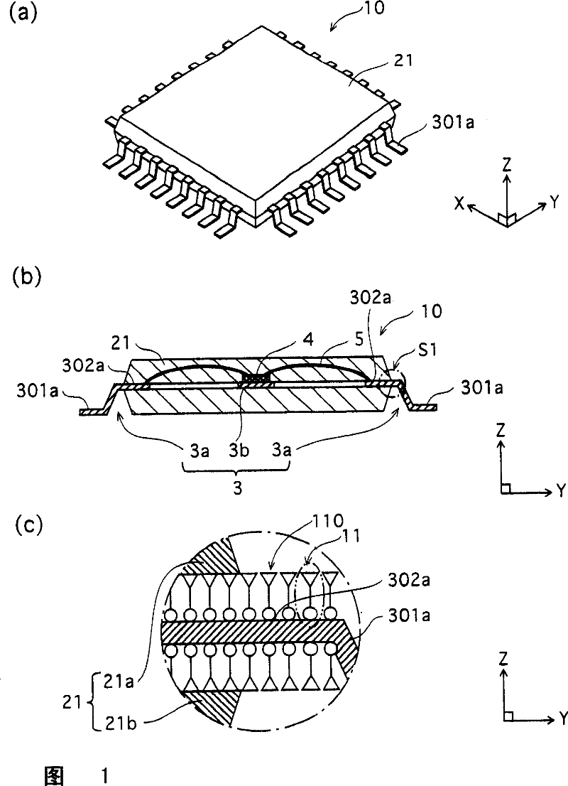
[0092] FIG. 1( a ) is an external perspective view showing the structure of a semiconductor device (QFP: Quad Flat Package 10 ) as an applied example of the present invention. Figure 1(b) is a yz cross-sectional view of QFP10. Fig. 1(c) is an enlarged view of the S1 portion in Fig. 1(b).

[0093] The QFP 10 is a surface mount type semiconductor device used for IC, LSI, etc., and includes a semiconductor chip 4, wiring leads 3, wires 5, molding resin 21, and the like.

[0094] The wiring lead 3 is made of a metal material having excellent electrical conductivity (copper alloy is mentioned as an example), and is made of a combination of chip pads 3 a and 3 b formed by pressing a metal plate.

[0095] QFP10 is a surface mount type semiconductor device, as shown in Figure 1 (a), has the following structure: a plate-shaped molding resin 21 having a square main surface with a certain thickness is formed, and extends from its periphery ...

Embodiment approach 2

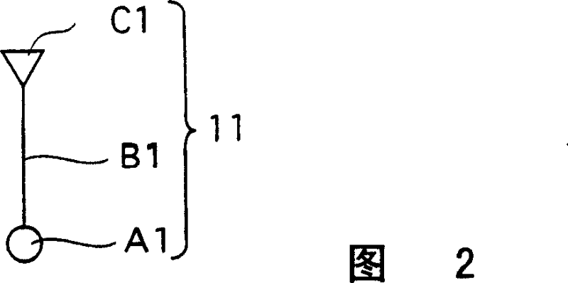
[0158] As described above, various effects can be exhibited by applying the organic film 110 composed of functional organic molecules 11 according to Embodiment 1 to a semiconductor device, but this is only an example, and the presence of a semiconductor chip is not essential. For example, it can be applied to an LED device having a light emitting diode element (LED) other than a semiconductor chip.

[0159] 7 is a schematic cross-sectional view showing the configurations of the wiring lead portion 30 and the reflector 22 of an LED device unit 31x according to Embodiment 2 of the present invention.

[0160] In this cross-sectional shape, the device unit 31x has a structure in which the wiring lead portion 30 is provided at the bottom of the mortar-shaped reflector 22 . The reflector 22 is formed by resin molding using a thermosetting resin material (epoxy resin or the like).

[0161] In such a device unit 31x, as in the first embodiment, the problem of resin burrs also occurs...

Embodiment approach 3

[0168] Embodiment 3 of the present invention will be described focusing on differences from Embodiment 2. FIG.

[0169] (Structure of LED device)

[0170] 8 is a cross-sectional view showing the structure and manufacturing steps of an LED device 31 according to Embodiment 3 of the present invention.

[0171] The basic structure of this LED device 31 includes a device unit 31x according to Embodiment 2, and as shown in FIG. The LED chip 42 is connected to the wiring lead portion 30 through a wire 53 .

[0172] In order to seal the LED chip 42 and the like, the reflector surface 201 and the exposed regions 301 and 302 in the reflector 22 are filled with a transparent sealing resin 82 .

[0173] Here, as the sealing resin 82, silicone resin which is an example of a thermosetting resin is used.

[0174] Here, in Embodiment 3 of the present invention, the organic film 120 composed of a monomolecular film formed by self-organization of the functional organic molecules 12 is forme...


PUM


Abstract

There is provided a semiconductor device that suppresses the occurrence of resin burrs and has favorable electrical connectivity and bond strength, and a manufacturing method for such semiconductor device. A resin-coated metal part is manufactured by forming an organic coating by depositing a material including functional organic molecules on a wiring lead composed of a metallic material. Each of the functional organic molecules includes a main chain, a first functional group having a metal bonding property, and a second functional group. The first functional group and the second functional group are provided at different ends of the main chain. Thereafter the functional organic molecules self-assemble by bonding of the first functional groups to metal atoms of the wiring lead. After performing the organic coating formation step, resin is adhered to a predetermined surface area of the wiring lead having the organic coating formed thereon.

Description

technical field [0001] The present invention relates to a wiring component, a resin-coated metal component, and a resin-sealed semiconductor device, and a method for manufacturing the resin-coated metal component and the semiconductor device. In particular, it relates to a technique for improving the adhesion between a metal material and a resin material. Background technique [0002] In semiconductor devices or wiring components, resin materials are widely used. [0003] Semiconductor devices such as integrated circuits (ICs) and large-scale integrations (LSIs) are generally manufactured by a method in which predetermined semiconductor elements are connected to wiring leads by wire bonding or the like, and a part of the wiring leads is exposed to the outside. Resin is adhered, and resin sealing is performed for encapsulation. [0004] 21 is a schematic cross-sectional view showing manufacturing steps of a resin-sealed QFP (quad flat package) type semiconductor device. [...

Claims


Application Information

Patent Timeline
Patent Type & Authority Applications(China)
IPC IPC(8): H01L21/48H01L21/50H01L21/56H01L21/60H01L23/488H01L23/498H01L23/31H01L33/00
CPCH01L2224/32245H01L2224/83192H01L2924/01005H01L2224/48247H01L2224/48091H01L2224/73265H01L2224/92247H01L2924/181
Inventor 福永隆博伊村领太郎
Owner PANASONIC HLDG CORP
Why Eureka
Try Eureka