

Wireless sensor network node device used for environmental monitoring
A wireless sensor and network node technology, applied in the direction of comprehensive factory control, comprehensive factory control, electrical program control, etc., can solve the problems of not fully adapting to the monitoring environment, short circuit of sensor nodes, inappropriate device selection, etc., to achieve low power consumption , Wide operating temperature range and reasonable structure
- Summary
- Abstract
- Description
- Claims
- Application Information
AI Technical Summary
Problems solved by technology
Method used
Image

Examples
Embodiment 1
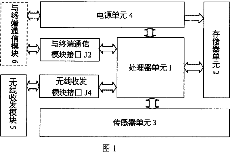
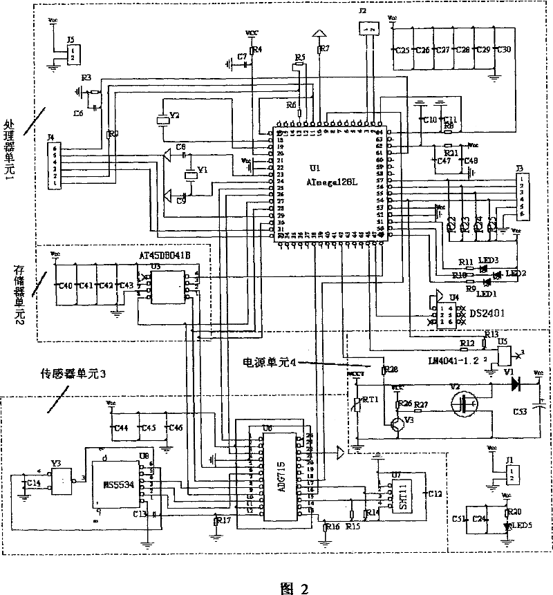
[0026] The aforementioned wireless sensor network node mainboard is implemented according to the structure shown in Fig. 1 and Fig. 2 . The motherboard mainly includes a processor unit 1 , a memory unit 2 , a sensor unit 3 and a power supply unit 4 . Single-chip microprocessor chip U1 selects ATmega128L, a high-end eight-bit single-chip microcomputer of AT Company. It has the following characteristics: the highest operating frequency is 8MHz, most instructions are completed in one cycle, and the calculation rate is high; on-chip 128kFlash, 4kSRAM and 4kEEPROM; support power-saving mode, power-down mode and other sleep modes; with a variety of buses and Sufficient input and output interfaces; with A / D, D / A interface; low voltage; small size. The random number generation chip U4 adopts DS2401 produced by Dallas Company, and is connected with the single-chip microprocessor chip U1. A random number is generated as a distinguishing identifier for each node. The temperature and h...
Embodiment 2
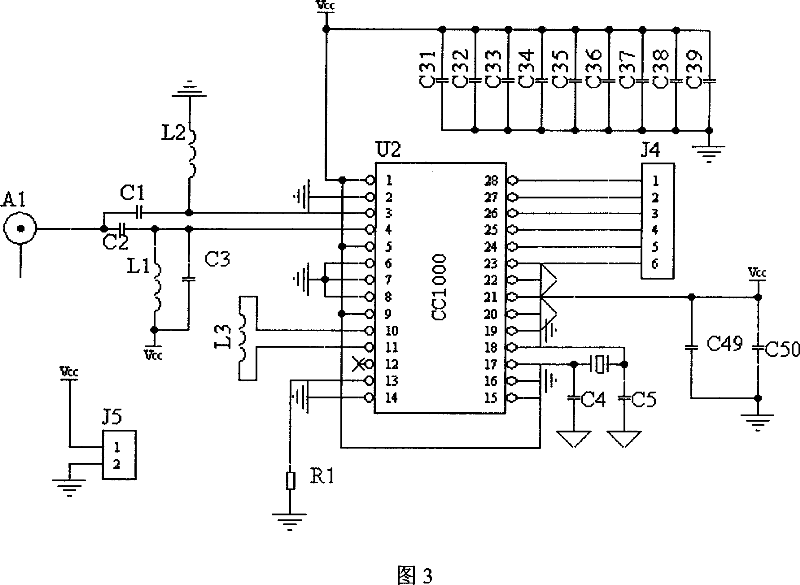
[0028] The above-mentioned wireless transceiver module 5 selects the CC1000 module of Chipcon Company, and its characteristics include: low power supply voltage: 2.3V-3.6V, extremely low power consumption, and the working frequency band is 315, 868, 915MHz. It is connected to the main board through the interface J4 of the wireless transceiver module and the power interface J5 of the wireless transceiver module. The interface J4 of the wireless transceiver module and the power interface J5 of the wireless transceiver module are made into two parts and distributed diagonally so as to be firmly installed on the main board. The interface J4 of the wireless transceiver module is a data line interface, and the power interface J5 of the wireless transceiver module is an interface of a power line and a ground wire. The antenna adopts a helical spring antenna, which is short and takes up less space and is not easy to be damaged.
Embodiment 3
[0030] The above-mentioned terminal communication module 6 mainly includes an "RS232" level conversion unit and a voltage conversion unit. The "RS232" level conversion chip U9 is MAX3317E from MAXIM Company, which has the following main features: 2.25V-3.3V power supply, ±15kV electrostatic protection, 1uA receiving effective shutdown mode, and 460kbps data transmission rate. The terminal communication module interface J2 is connected with the "RS232" level conversion chip U9, and the "RS232" level conversion chip U9 is connected with the "RS232" interface J7. Since this module generally does not work on site and does not have to be set up with the nodes (it is only used when individual nodes communicate effectively with the terminal or when the terminal programs the node before the node is deployed), the mechanical strength and adaptability to the environment are required not tall. You can choose to use the rechargeable battery on the node to supply power, or you can convert...
PUM
 Abstract
Description
Claims
Application Information