
Micro-electromechanical inductor for suppressing the substrate eddy effect and its manufacture method

A technology of micro-electronic machinery and eddy current effect, applied in the manufacture of inductors/transformers/magnets, inductors, fixed inductors, etc., can solve the problems of difficult to exceed the quality factor of inductors, increase the cost and design difficulty, and achieve the suppression of eddy currents in the substrate effect, reduce substrate loss, obvious effect

Inactive Publication Date: 2007-10-24
SOUTHEAST UNIV
View PDF0 Cites 16 Cited by
  • Summary
  • Abstract
  • Description
  • Claims
  • Application Information

AI Technical Summary

Problems solved by technology

[0003] Through the retrieval of prior art documents, it is found that the current implementation of inductors that suppress the eddy current effect of the substrate is similar to the literature Olive H. Murphy, Kevin G. McCarthy, Design of Multiple-Metal Stacked Inductors Incorporating an Extended PhysicalModel, IEEE Trans. Microw. The metal wire interconnection process used in Theory Tech., vol.53, no.6, pp.2063-2072, Jun.2005. (Design and physical model of multilayer metal interconnection inductors) grounds the shield under the inductor structure, This increases the cost and design difficulty and the quality factor of the inductor is difficult to exceed 15

Method used


Image

  • Micro-electromechanical inductor for suppressing the substrate eddy effect and its manufacture method
  • Micro-electromechanical inductor for suppressing the substrate eddy effect and its manufacture method
  • Micro-electromechanical inductor for suppressing the substrate eddy effect and its manufacture method

Examples


Embodiment Construction

[0036] specific implementation plan

[0037] The practical application of the steps of the present invention will be described in detail below in conjunction with the accompanying drawings.

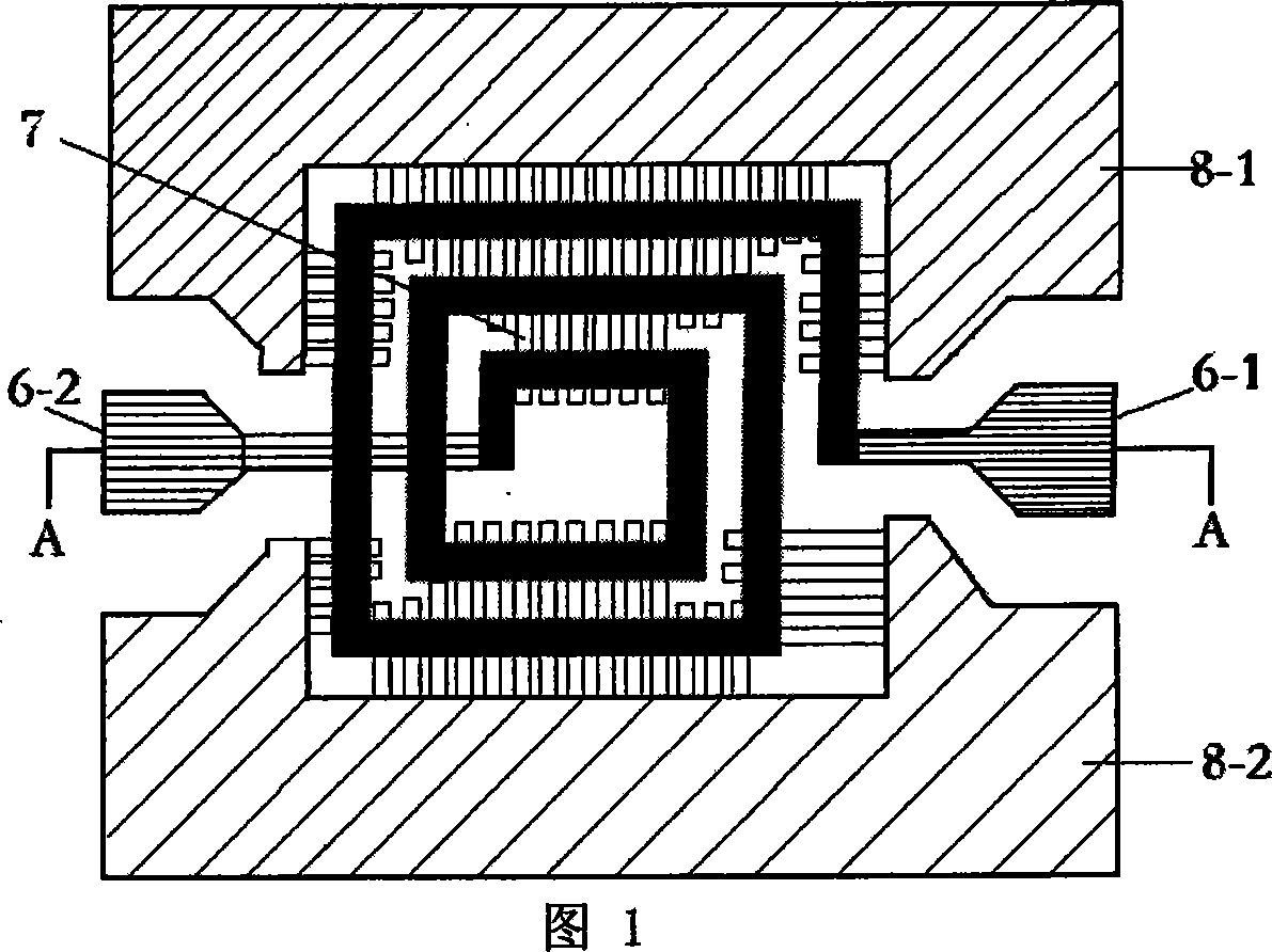
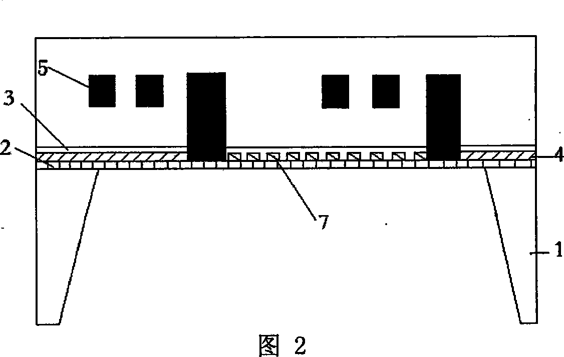
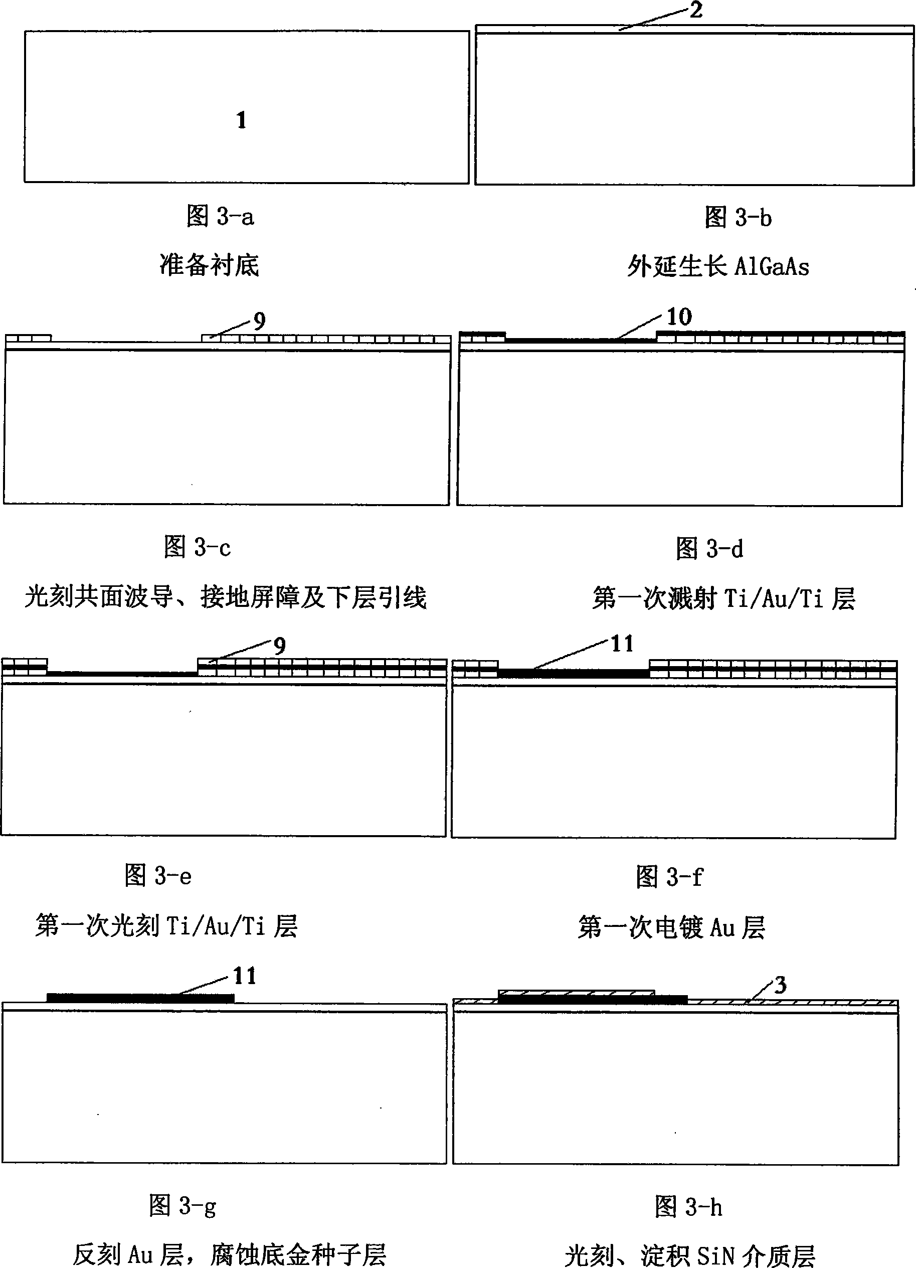
[0038] As shown in Fig. 1 and Fig. 2, it is the schematic diagram of the micromechanical inductor prepared by the method of the present invention, comprising gallium arsenide (GaAs) substrate 1, aluminum gallium arsenide (AlGaAs) thin film 2, silicon nitride (SiN) dielectric layer 3 , Inductor lower lead wire 4, inductor upper coil 5, first coplanar waveguide signal line 61, second coplanar waveguide signal line 62, ground barrier 7 and first coplanar waveguide ground wire 81, second coplanar waveguide ground wire 82 The inductance is based on a GaAs substrate 1, a layer of AlGaAs thin film 2 is arranged on the upper surface of the GaAs substrate 1, and a layer of SiN dielectric layer 3 is arranged on the upper surface of the AlGaAs thin film 2, and the upper layer coil 5 of the inductor ...


PUM


Abstract

The MEMS-based inductance comprises: a GaAs (1) substrate, one layer of AlGaAs film (2) on top surface of (1), a SiN medium layer (3) on top surface of (2), a top ring (5) hanging above (3), the center of (5) connecting with the bottom wire (4) on (2), the outer insulation part of (5) connecting with the first coplanar waveguide signal wire (61), a grounding barrier (7) between (5) and (3) connecting with the inner side of coplanar waveguide grounding wire, and all of the coplanar waveguide signal lines (61, 62) and grounding lines (81, 82) together forming the coplanar waveguide transmission line. This invention can inhibit the vortex effect in substrate.

Description

technical field [0001] The invention provides a micro-electromechanical inductor capable of suppressing the eddy current effect of a substrate based on a coplanar waveguide transmission line and a preparation method thereof, belonging to the technical field of micro-electromechanical systems. Background technique [0002] In the field of microwave communication, coplanar waveguide transmission lines can be easily connected to external components, such as resistors, capacitors, and inductors to form microwave circuits. This type of transmission line does not need to have holes on the substrate like microstrip lines, so it is more and more widely used in microwave integrated circuits. At the same time, inductance with high quality factor in microwave integrated circuits is very important, it can greatly reduce the phase noise or power loss of oscillators and amplifiers, and make matching networks and filters have lower losses. The quality factor of an inductor is defined as t...

Claims


Application Information

Patent Timeline
IPC IPC(8): H01F17/00H01F41/00H01P3/00H01L27/00H01L21/70
Inventor 廖小平武锐
Owner SOUTHEAST UNIV
Learn More