Process for reversing pure-golden Au alloy bonding LED

A technology of alloy bonding and pure gold, which is applied in the direction of electrical components, circuits, semiconductor devices, etc., can solve the problems of reduced light output efficiency, reduced reliability, and high junction temperature of devices, so as to improve stability and yield, and optimize heat dissipation , Improve the effect of stability and yield

Inactive Publication Date: 2007-11-21
AQUALITE CO LTD
View PDF0 Cites 9 Cited by
  • Summary
  • Abstract
  • Description
  • Claims
  • Application Information

AI Technical Summary

Problems solved by technology

Under rated working conditions, high resistance will cause excessive heat generated by the LED, which will lead to excessive junction temperature of the device, reduced light extraction efficiency and reduced reliability of the device.

Method used


Image

  • Process for reversing pure-golden Au alloy bonding LED
  • Process for reversing pure-golden Au alloy bonding LED
  • Process for reversing pure-golden Au alloy bonding LED

Examples


preparation example Construction

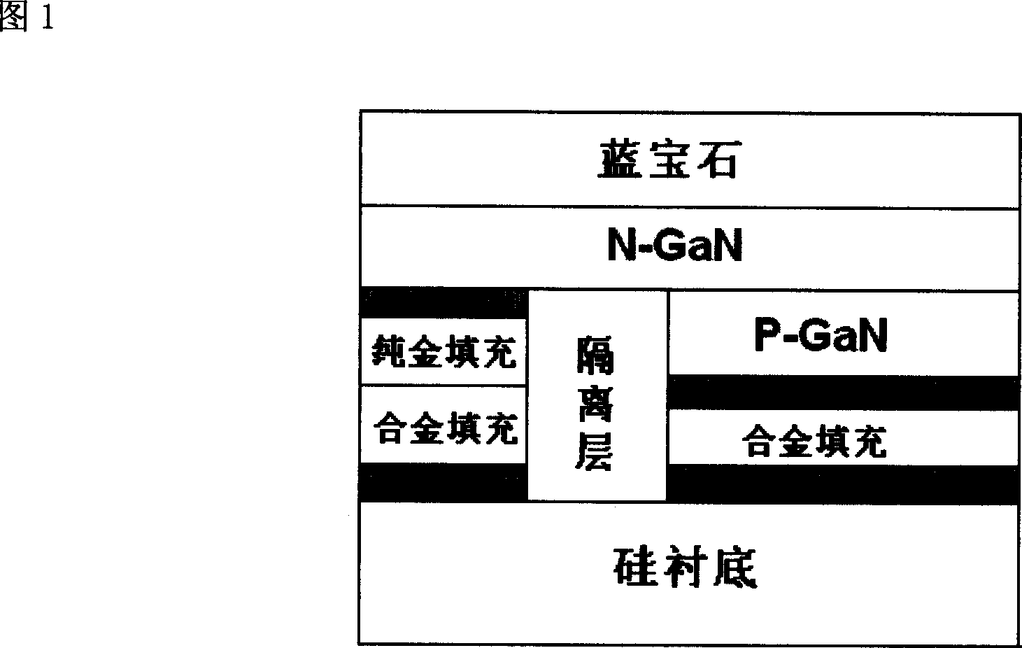
[0034] In order to prepare the above-mentioned pure gold Au alloy bonded LED flip chip, the preparation method of the present invention comprises the following steps:

[0035] First, use MOCVD (metal organic chemical vapor deposition) equipment to epitaxially grow GaN-based high-power LED structure epitaxial wafers, and the substrate is sapphire (Al 3 o 2 ). Then etch the steps of the N surface and the scribe line of the chip size to expose the N-GaN mesa, so as to be used as the N electrode and the welding pad. The N-type mesa is etched by reactive ion etching equipment RIE, and the reaction gas is Cl:Ar=10:3.

[0036] Using ICP (Coupled Plasma Etching) or RIE (Reactive Ion Etching) equipment to dry-etch the P-GaN layer and the light-emitting layer with chlorine ions and argon ions, and make the P-GaN layer and the light-emitting layer The underlying N-GaN layer forms the electrical contact and is etched with photoresist or SiO 2 Make a mask.

[0037] Afterwards, a layer...

Embodiment 1

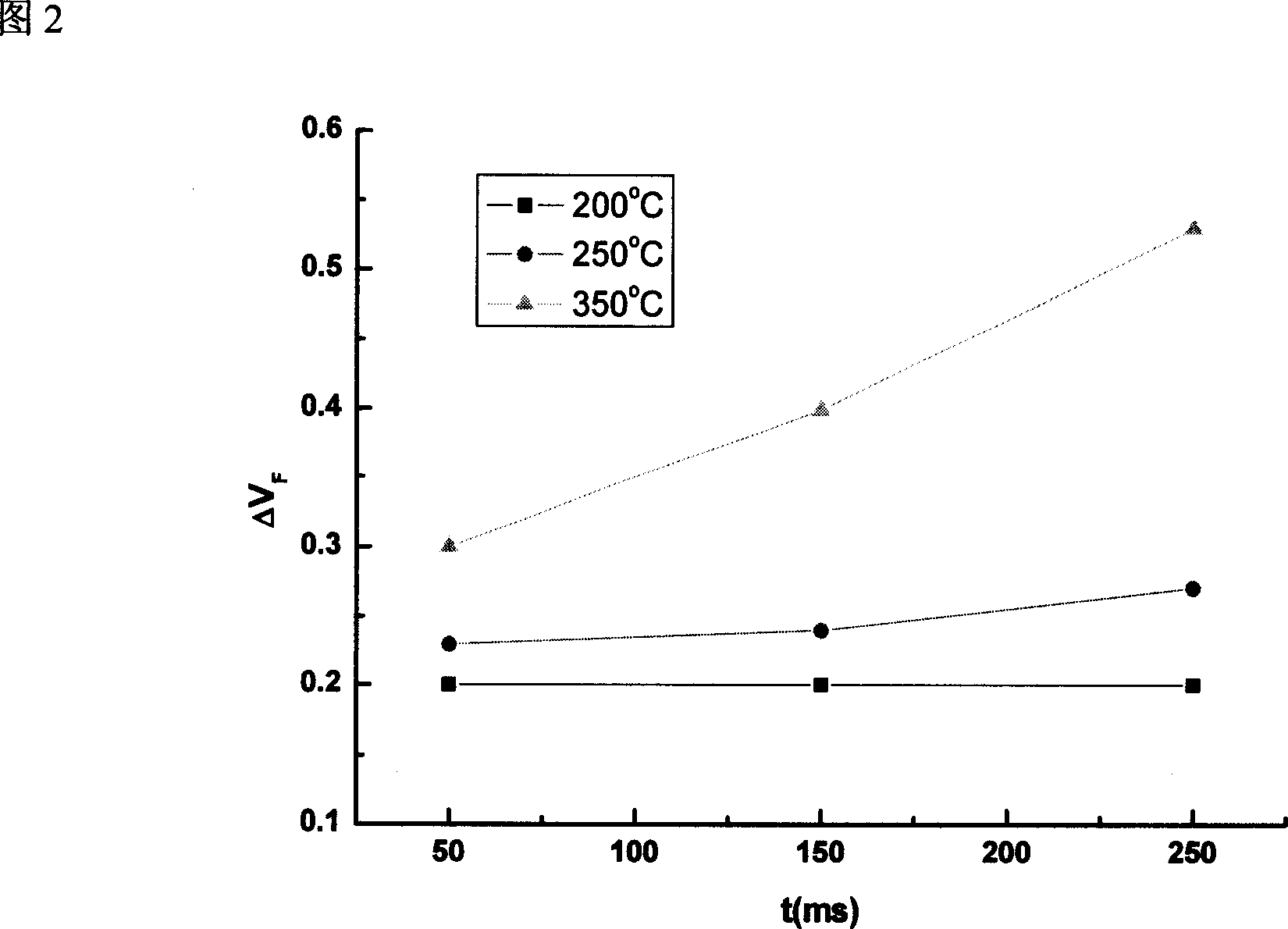
[0042] Embodiment 1, adjust the welding temperature and time.

[0043] The process parameters for welding the LED chip and the silicon substrate together are as follows:

[0044] The heating and bonding temperature is controlled at 200°C to 350°C, and the welding time is adjusted within a range of 50ms to 250ms. From Figure 2, it can be seen that under the premise that the welding temperature parameters remain unchanged, the grain V measured by adjusting the welding time F (Forward voltage) difference between each other ΔV F . Among them, when the soldering temperature is 200°C, the difference ΔV F Only 0.2V. When the soldering temperature increases, the difference ΔV F increase, and when the welding temperature is higher, at 350°C, the difference ΔV F It increases significantly with the increase of welding time.

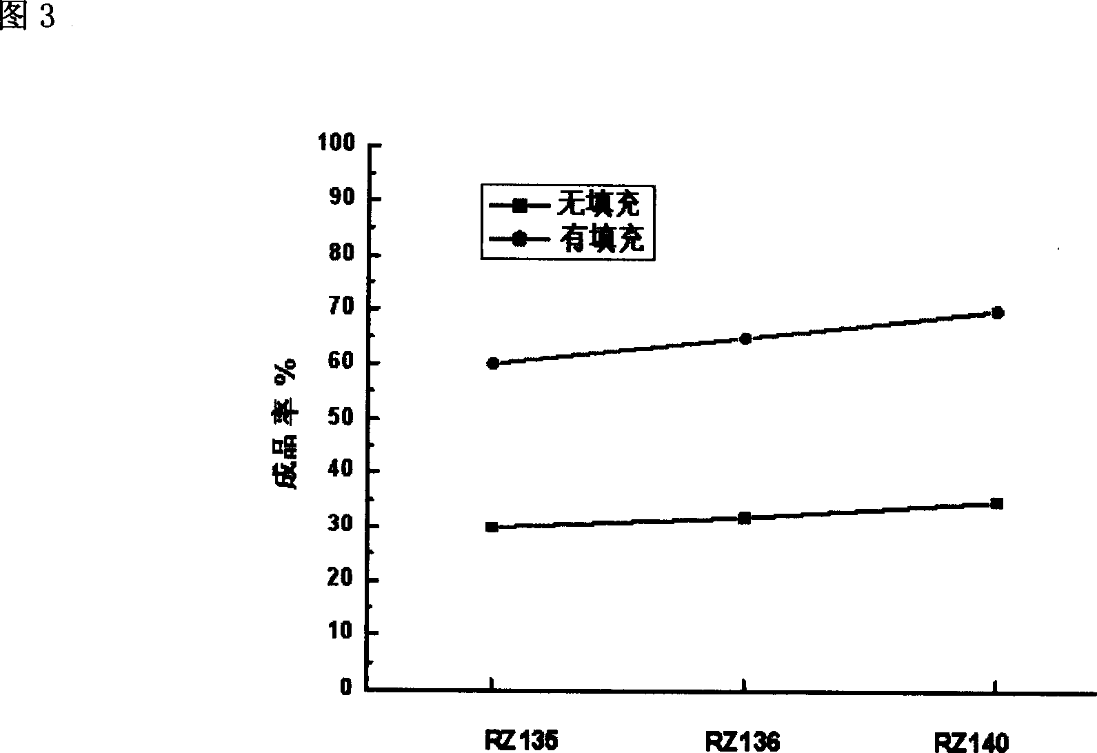
[0045] FIG. 3 is a comparison of the yield of the flip chip of the invented technology (with filling) and the flip chip of the prior art (without filling). ...


PUM

PropertyMeasurementUnit
thicknessaaaaaaaaaa
thicknessaaaaaaaaaa

Abstract

This is a process method of a pure Au and alloy LED. It is composed by a P-N expending slice, pure Au filling layer, alloy filling layer and a silicon underlay of reflection layer. The P-N expending slice includes a sapphirine underlay, a N-GaN layer on the underlay, a P-GaN layer on the N-GaN layer and a reflection layer in between. A metal layer which is good for current diffusion is deposited on the P-GaN layer. A P/N electrode is led from the P-GaN layer and the N-GaN layer separately. An isolation layer is formed in between the P/N electrode. An electric insulation layer is formed on a silicon underlay, to the top formed a metal reflection layer. The P-N expending slice is heat jointed with the silicon underlay by filling in pure Au and alloy.

Description

technical field [0001] The invention relates to a manufacturing process method of a semiconductor device, in particular to a method for preparing a pure gold Au alloy-bonded LED flip-chip (Flip-Chip). Background technique [0002] Light-emitting diode LED technology has developed to the present, and the improvement of unit luminous flux allows it to enter the field of lighting, which is called semiconductor lighting. Semiconductor lighting is a real revolution in lighting technology in the past century. Since semiconductor materials directly convert electrical energy into light, the biggest difference between semiconductor lighting and traditional lighting sources is that its light does not generate heat. However, the process of improving the luminous flux of high-power LEDs is accompanied by technical bottlenecks in heat dissipation. The success of heat dissipation treatment directly affects the optical parameters of semiconductor lighting and the life expectancy of product...

Claims


Application Information

Patent Timeline
Patent Type & Authority Applications(China)
IPC IPC(8): H01L33/00H01L33/10H01L33/14H01L33/36
Inventor 董志江靳彩霞黄素梅姚雨
Owner AQUALITE CO LTD
Why Eureka
Try Eureka