Processing method for silicon sheet surface

A treatment method and silicon wafer surface technology, applied to electrical components, climate sustainability, circuits, etc., can solve problems such as poor repeatability, uneven corrosion, pollution, etc., to simplify process steps, improve uneven corrosion, Improved repeatability and consistency

Inactive Publication Date: 2008-01-16
SEMICON MFG INT (SHANGHAI) CORP +1
View PDF1 Cites 13 Cited by
  • Summary
  • Abstract
  • Description
  • Claims
  • Application Information

AI Technical Summary

Problems solved by technology

[0008] The invention provides a method for treating the surface of a silicon wafer. The method uses a new mixed solution to treat the surface of the silicon wafer to increase the light absorption rate of the surface of the silicon wafer, improve t

Method used


Image

  • Processing method for silicon sheet surface
  • Processing method for silicon sheet surface
  • Processing method for silicon sheet surface

Examples


Example Embodiment

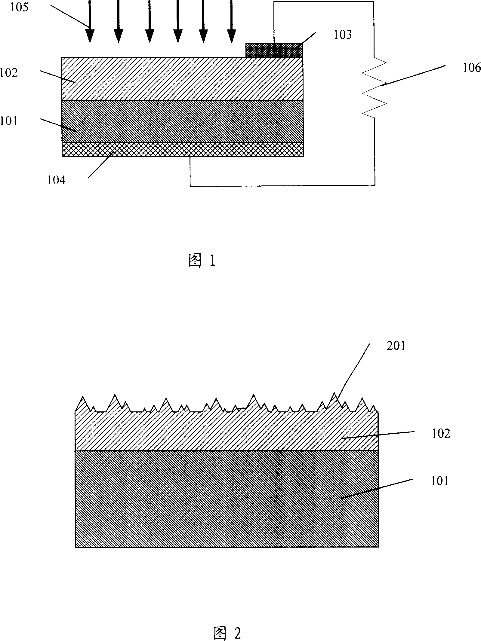
[0037] In order to make the above objectives, features and advantages of the present invention more obvious and understandable, the specific embodiments of the present invention will be described in detail below with reference to the accompanying drawings.

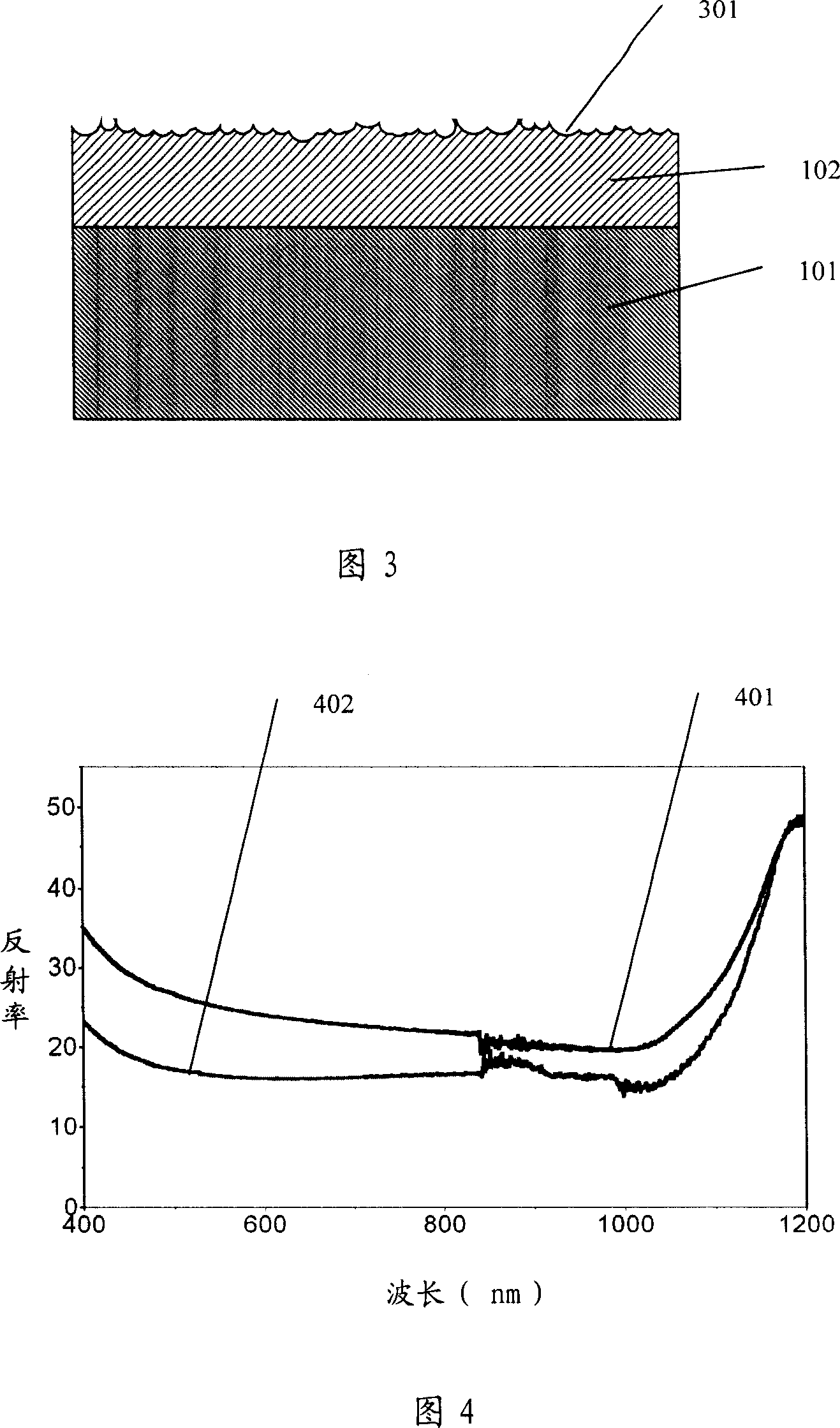
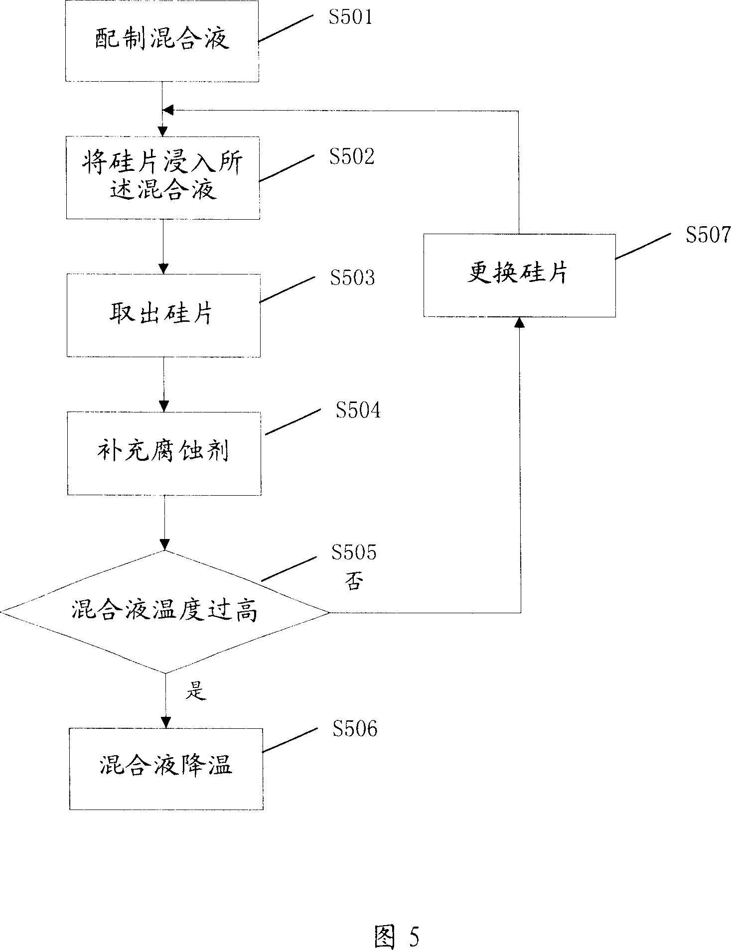
[0038] The silicon wafer surface treatment method of the present invention uses a mixed solution with a new formula to treat the surface of the silicon wafer, which can remove the damaged layer on the surface of the silicon wafer, and can also form a suede on the surface of the silicon wafer, thereby improving the efficiency of the device. The mixed liquid in the present invention contains hydrogen fluoride (NH 4 HF 2 ), potassium nitrate (KNO 3 ) And sulfuric acid (H 2 SO 4 ). In the present invention, the amount of each component in the mixed solution in the initial preparation is called the preparation amount, and the molar ratio of the preparation amount of each component is: 1% to 20% KNO 3 , 5% to 30% NH 4 HF 2 , And 50%...


PUM


Abstract

The invention discloses a processing method of silicon surface. The method makes roughening treatment on the surface of silicon with new compound liquid to lower the surface reflection rate and remove the cutting damage layer formed when the silicon is cut from silicon ingot, thus greatly improving the conversion efficiency of silicon solar energy battery and effectively solving problems of uneven corrosion, poor repetition, and environmental pollution in the current roughening treatment on the surface of silicon. In addition, the invention also has the advantages of simple technique and low cost.

Description

technical field [0001] The invention relates to the technical field of semiconductor manufacturing, in particular to a method for treating the surface of a silicon wafer used to manufacture solar cells. Background technique [0002] A solar cell is a device that uses the photovoltaic effect to directly convert sunlight energy into electrical energy. Figure 1 is a schematic diagram of the structure of a solar cell. As shown in Figure 1, a solar cell is mainly composed of an n-type semiconductor material 101 and a p-type semiconductor material 102, and an upper electrode 103 and a lower electrode 104 are respectively made on both sides to draw electric energy, wherein, in order to absorb light radiation 105, the upper electrode The metal is usually made into a free grid pattern (open grid pattern) to facilitate light absorption. In operation, optical radiation 105 impinges on the semiconductor, part of which is reflected and part is received by the crystal. When the energy ...

Claims


Application Information

Patent Timeline
IPC IPC(8): H01L21/306H01L31/18C23F1/10C23F1/24
CPCY02P70/50
Inventor 苏晓平江彤
Owner SEMICON MFG INT (SHANGHAI) CORP
Why Eureka
Try Eureka