Pressure capacitance type sensor substrate cavity-forming method

A sensor and pressure-capacitance technology, applied in the field of microelectronic machining, can solve the problems of low precision, cumbersome process, and low yield, and achieve the effects of high selection ratio, wide process manufacturing window, and low device damage

Inactive Publication Date: 2008-01-30
杭州科岛微电子有限公司 +1
View PDF0 Cites 15 Cited by
  • Summary
  • Abstract
  • Description
  • Claims
  • Application Information

AI Technical Summary

Problems solved by technology

[0003] The present invention aims to solve the problems of low precision, high cost, cumbersome process, and low yield rate caused by wet etching of the substrate micromachined into the cavity of the pressure capacitive sensor. Therefore, the pressure capacitive sensor base of the present invention is provided. Chip cavity forming method, using this method to process the substrate into a cavity, with high processing precision, simple operation, low cost, stable product performance, and high yield

Method used


Image

  • Pressure capacitance type sensor substrate cavity-forming method
  • Pressure capacitance type sensor substrate cavity-forming method

Examples


Embodiment Construction

[0033] The cavity forming method of the pressure capacitive sensor substrate adopts the following steps:

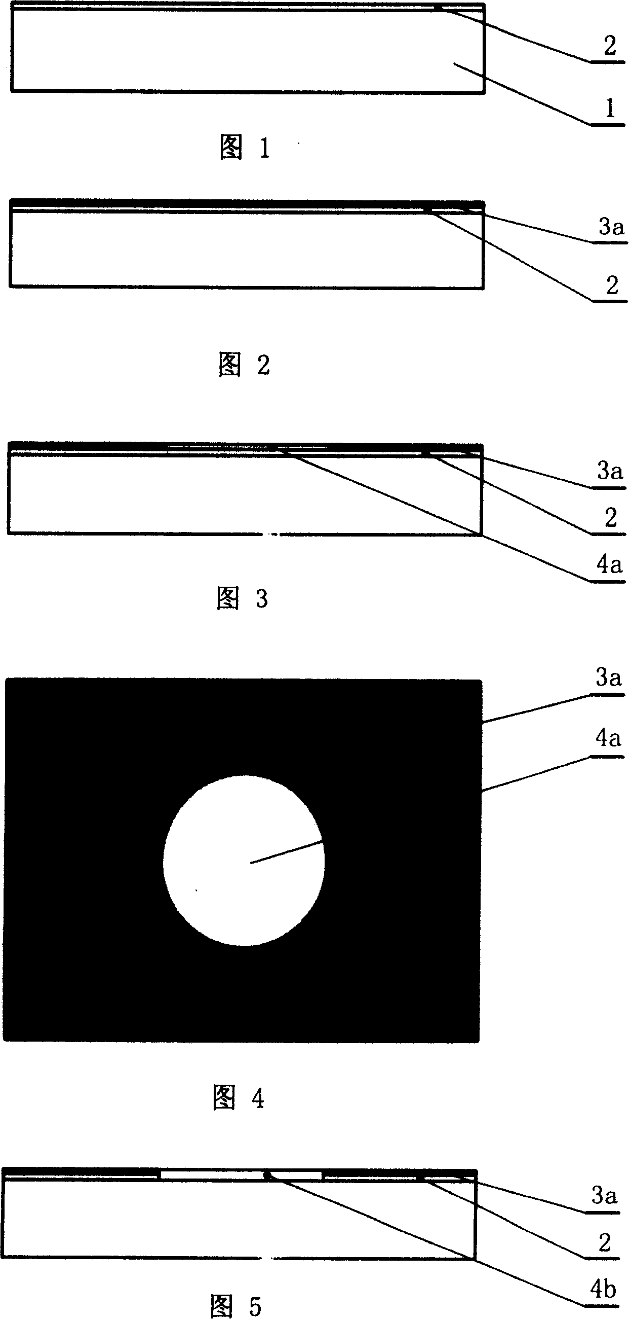
[0034] ① Select a silicon wafer 1 with a thickness of 500 microns, wash and remove surface organic matter, transition metals, alkaline ions and particles, etc., and prepare a layer 2 by dry oxygen-wet oxygen-dry oxygen method in a KL45-Φ180 4-tube diffusion furnace Micron to 2.5 micron thick silicon dioxide layer 2, wherein dry oxygen is 15-20 minutes, wet oxygen is 8-10 hours, as shown in Figure 1;

[0035] ② coat positive BP212 photoresist layer 3a on silicon dioxide layer 2, obtain the thing shown in Fig. 2, use H94-25G type photolithography machine photolithography, form the circular microstructure concave cavity I4a of diameter 400 microns The material on the bottom surface is silicon dioxide, as shown in Figure 3 and Figure 4;

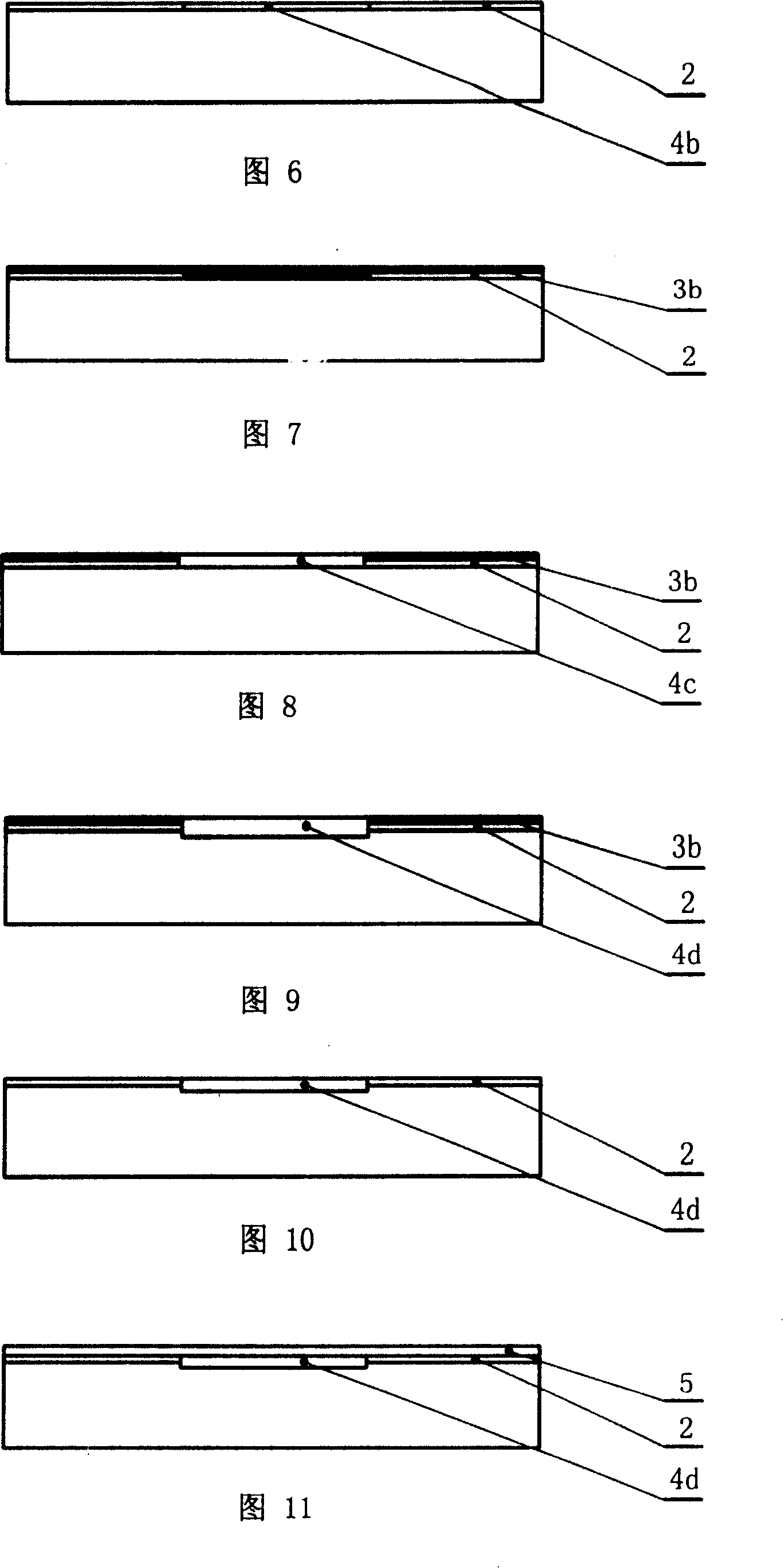
[0036] ③Using the photoresist layer 3a as a mask, use an ICP-2B type plasma etching machine to etch the silicon dioxide layer in the micro...


PUM

PropertyMeasurementUnit
thicknessaaaaaaaaaa
thicknessaaaaaaaaaa
diameteraaaaaaaaaa

Abstract

A substrate cavitation method for the pressure volume sensor has the advantages of high precision, low cost, easy operation and stable quality. The method includes the following steps: (1) forming a silica layer formed by the oxidation on one surface of the selected silicon; (2) coating a photoresist layer on the silica layer and forming a micro structure concave cavity I after exposing and developing, and the material at the bottom of the micro structure concave cavity I is silica; (3) etching the silica layer in the micro structure concave cavity I by means of ICP plasma-etching, and the photoresist layer is the mask, forming a micro structure concave cavity II, the material at the bottom of which is silicon; (4) removing the photoresist layer; (5) coating the photoresist layer again and forming a micro structure concave cavity III corresponding to the micro structure concave cavity II after exposing and developing; (6) etching the silicon wafer to a certain depth in the micro structure concave cavity III by means of ICP plasma-etching, and the photoresist layer is the mask; (7) removing the photoresist layer and obtaining the substrate provided with a micro structure concave cavity IV. The invention is suitable for making the substrate of the depressor sensor.

Description

technical field [0001] The invention relates to a micro-electro-machining method, in particular to a micro-machining manufacturing method for a sensor. Background technique [0002] Pressure sensors are widely used in process control, environmental control and pneumatic equipment. Silicon micro pressure sensor is a new type of product developed on the basis of microelectronics technology. Microelectromechanical systems (MEMS) have many advantages that traditional electromechanical technologies do not have, including general reduction in mass and size, mass production, low production costs and energy consumption, easy fabrication of large-scale and multi-mode array etc. Silicon micro pressure sensors are usually divided into piezoresistive and piezocapacitive. At present, most silicon sensors are piezoresistive sensors. The production of piezocapacitive sensors is rare in China, and the micromachining process of piezocapacitive sensors In general, wet etching is used to et...

Claims


Application Information

Patent Timeline
Patent Type & Authority Applications(China)
IPC IPC(8): H01L21/3065B81C1/00G01L9/12G01L1/14
Inventor 赵玉成陈旭远
Owner 杭州科岛微电子有限公司
Why Eureka
Try Eureka