

Cleaning liquid composition for plasma etching residues in semi-conductor industry
A technology for etching residues and cleaning solutions, applied in detergent compositions, organic detergent compositions, non-surface-active detergent compositions, etc., can solve the problem of inability to simultaneously control metal and non-metal etching rates, channel feature size changes, Change the semiconductor structure and other issues to achieve good applicable environment and effect, good corrosion inhibition effect, and environmental safety effect
Inactive Publication Date: 2008-02-20
ANJI MICROELECTRONICS (SHANGHAI) CO LTD
View PDF4 Cites 8 Cited by
- Summary
- Abstract
- Description
- Claims
- Application Information
AI Technical Summary
Problems solved by technology
This type of cleaning solution usually cannot control the etching rate of metals and non-metals at the same time. After cleaning, it is easy to change the characteristic size of the channel, thereby changing the semiconductor structure; and because of its large etching rate, the cleaning operation window is very small. can have various negative effects
[0004] The inhibitors used in the prior art have pyrocatechol and pyroglucinol. On the one hand, these inhibitors cannot simultaneously control the etching rate of metals and oxides; on the other hand, they have a strong effect on the environment and human beings.
Method used
View moreImage
Smart ImageViewing Examples

Examples
Embodiment 1
[0039] Components of cleaning solution composition 1: N-methylpyrrolidone 60wt%, DI 28.44wt%, NH 4 F 1.25wt%, Ac 1.56wt%, AcNH 4 7.8wt%, 0.3wt% benzotriazole (BTA), ammonium polyacrylate (molecular weight: 600), 0.15wt%, G 0.5wt%.
Embodiment 2
[0041] Components of cleaning solution composition 2: N-methylpyrrolidone 50wt%, DI 26.3wt%, NH 4 F 3wt%, Ac 5.1wt%, AcNH 4 12.4wt%, benzotriazole (BTA) 0wt%, ammonium polyacrylate (molecular weight: 600), 0.3wt%, G 0.2wt%.
Embodiment 3
[0043] Components of cleaning liquid composition 3: N-methylpyrrolidone 85wt%, DI 8wt%, NH 4 F0.05wt%, Ac 1wt%, AcNH 4 1wt%, benzotriazole (BTA) 0.94wt%, ammonium polyacrylate (molecular weight: 600), 00.01wt%, G 4wt%.
Login to View More PUM
 Abstract
The invention discloses a cleaning liquid combination used for removing plasma-etching residue in semiconductor industry. The cleaning liquid comprises amount of solvent used for effectively washing, buffer aqueous solution, fluoride, antifreeze agent, polymer inhibitor. The cleaning liquid combination of the invention can effectively clean plasma-etching residue in semiconductor industry without eroding SiO2, PETEOS, silicon, low medium material and some metals such as Ti, Al and Cu.
Description
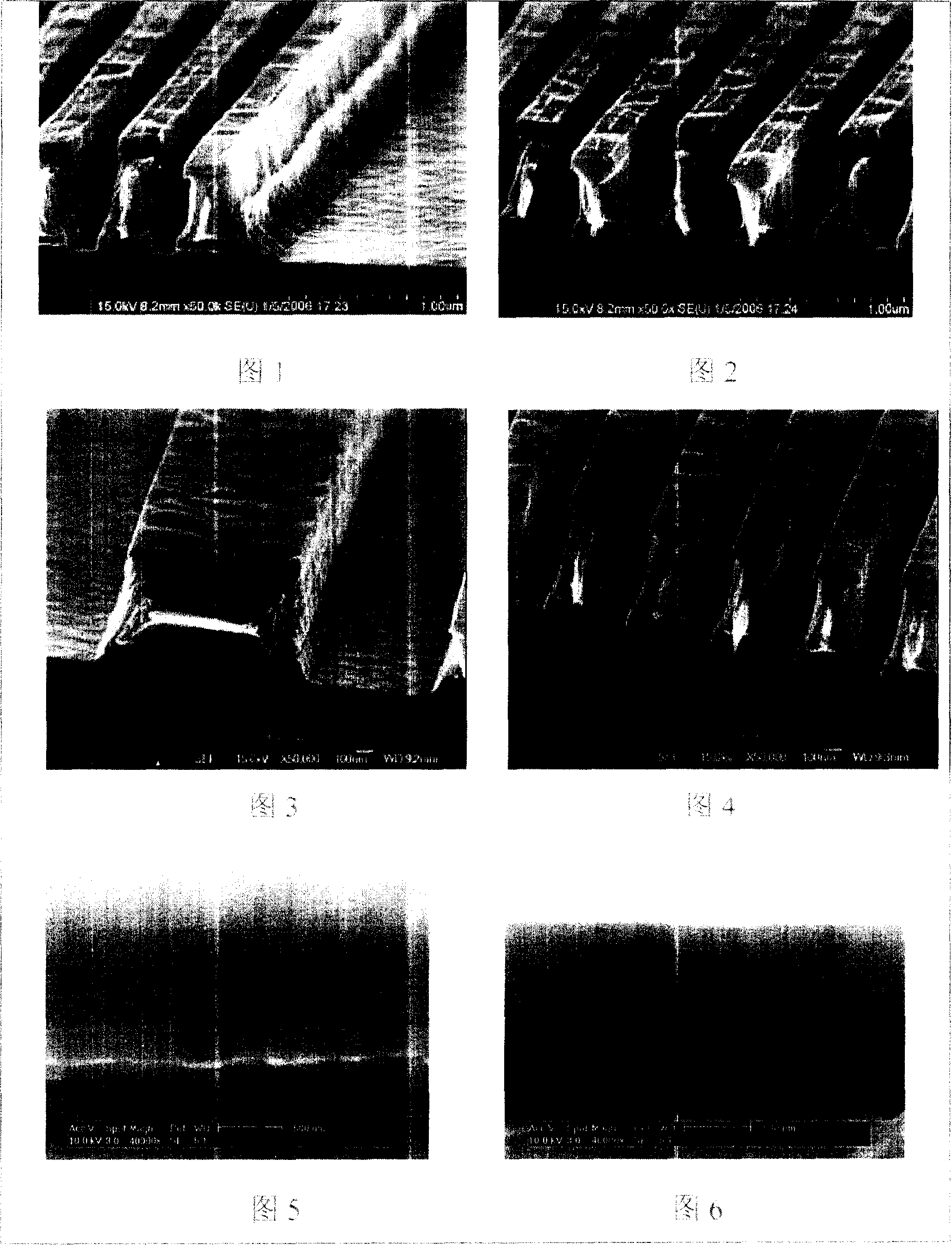
technical field [0001] The invention relates to a cleaning liquid composition, in particular to a cleaning liquid composition used for plasma etching residues in the semiconductor industry. Background technique [0002] In the manufacturing process of semiconductor components, the coating, exposure and imaging of photoresist layers are necessary process steps for the pattern manufacturing of components. Residues of photoresist material need to be completely removed at the end of patterning (ie, after photoresist coating, imaging, ion implantation, and etching) before proceeding to the next process step. Ion bombardment during the doping step hardens the photoresist polymer, thus making the photoresist less soluble and thus more difficult to remove. To date, a two-step process (dry ashing and wet etching) has generally been used in the semiconductor manufacturing industry to remove this photoresist film. The first step uses dry ashing to remove most of the photoresist layer...
Claims
Login to View More Application Information
Patent Timeline
 Patent Type & AuthorityApplications(China)
IPC IPC(8): C11D7/34H01L21/302C11D7/32
CPCC11D7/10C11D7/50C11D3/37C11D11/0047H01L21/02057C11D3/3761C11D7/261C11D7/265C11D7/5004C11D2111/22
Inventor刘兵彭洪修王淑敏
OwnerANJI MICROELECTRONICS (SHANGHAI) CO LTD