
Multi-wave length parallel buffer full optical buffer

An optical buffer and multi-wavelength technology, applied in the field of optical communication, can solve problems such as signal quality degradation, achieve good buffer performance, improve signal-to-noise ratio, and maximize flexibility

Inactive Publication Date: 2008-02-20
BEIJING JIAOTONG UNIV
View PDF0 Cites 23 Cited by
  • Summary
  • Abstract
  • Description
  • Claims
  • Application Information

AI Technical Summary

Problems solved by technology

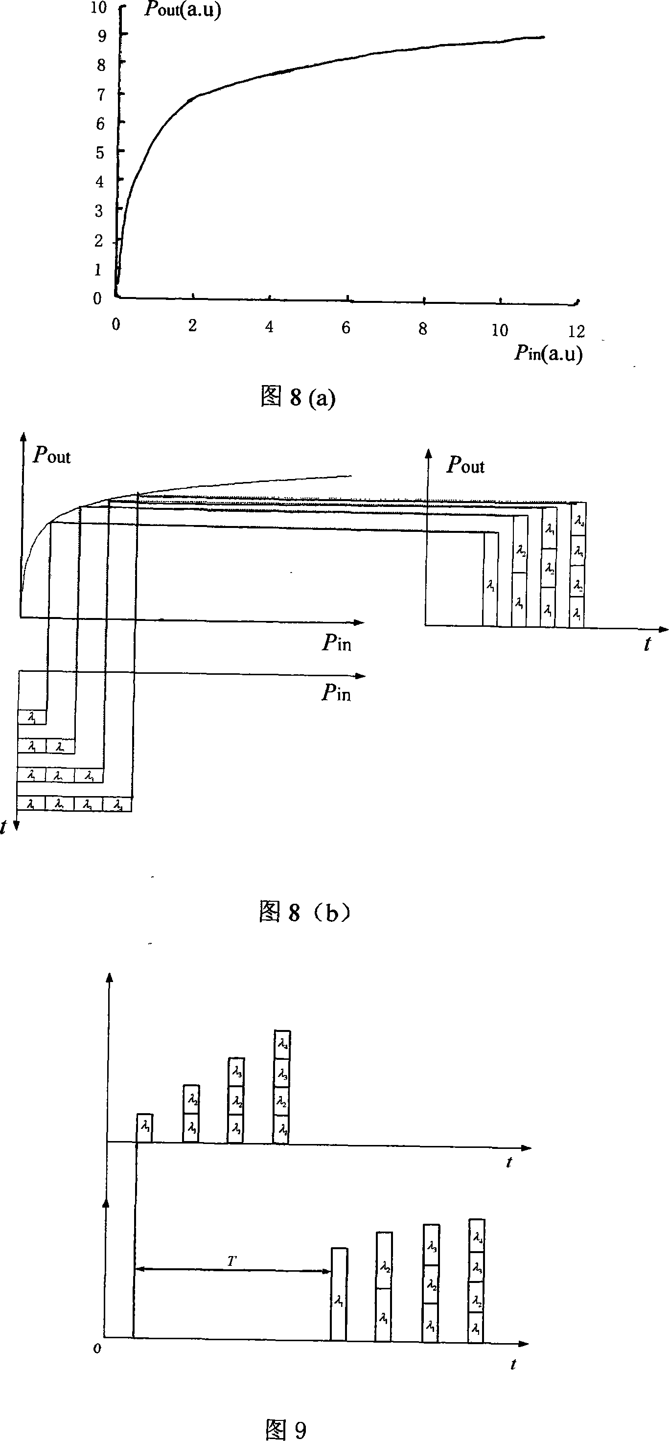
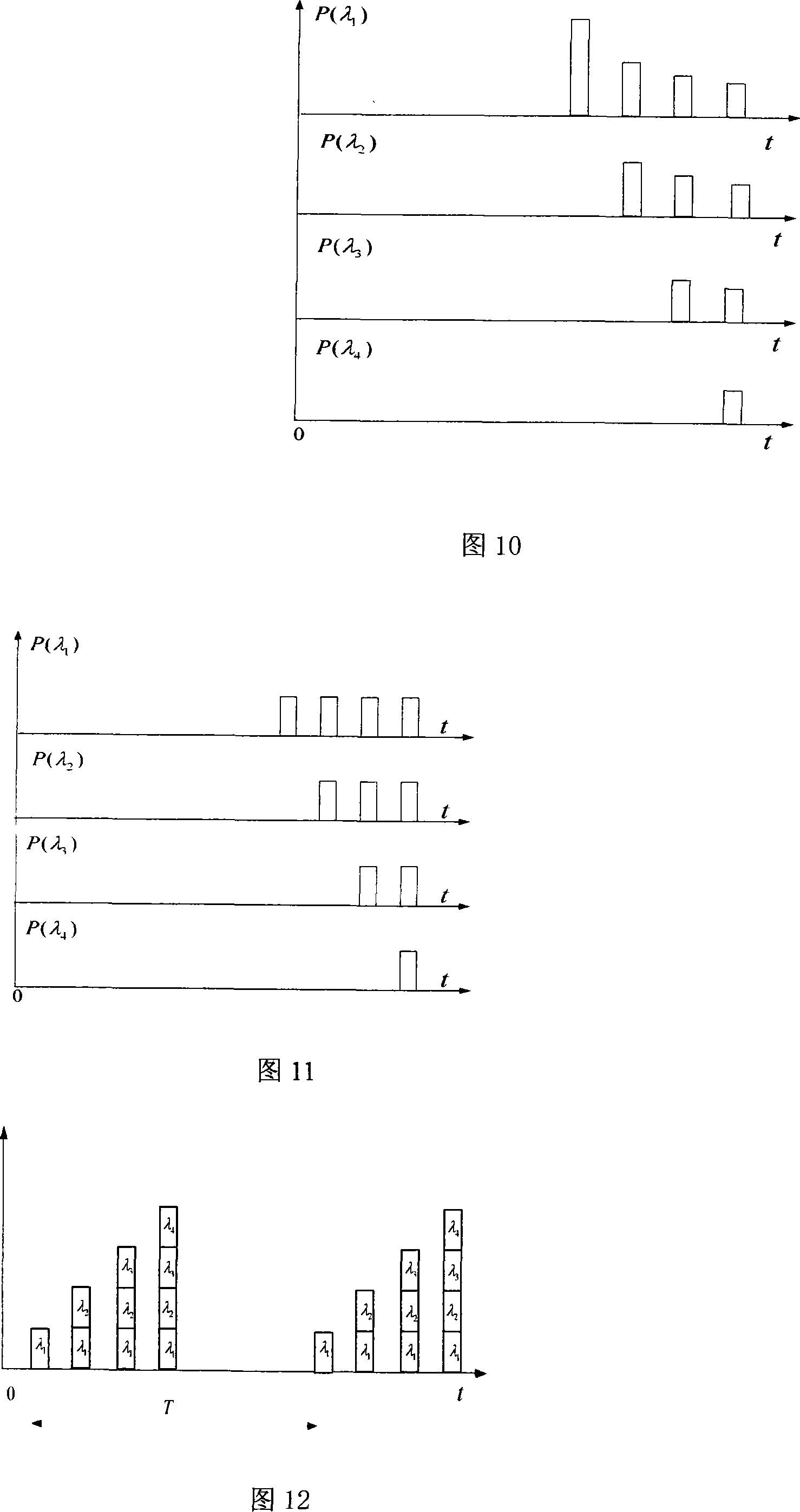
The phenomenon that the total power of the synthesized signal varies in a large range leads to a serious decline in signal quality. Therefore, the problem of power balance during multi-wavelength buffering must be well solved, and this is the technical problem to be solved by the present invention

Method used


Image

  • Multi-wave length parallel buffer full optical buffer
  • Multi-wave length parallel buffer full optical buffer
  • Multi-wave length parallel buffer full optical buffer

Examples


Embodiment 1

[0037]The power equalizer 1 and the power equalizer 4 groups (they are composed of the same kind of devices) are semiconductor optical amplifiers SOA, which have obvious gain saturation characteristics. The buffer unit 3 uses the inventor's patented product "dual-loop coupled all-optical buffer" (Patent No. ZL 02 1 53429.2, 2002).

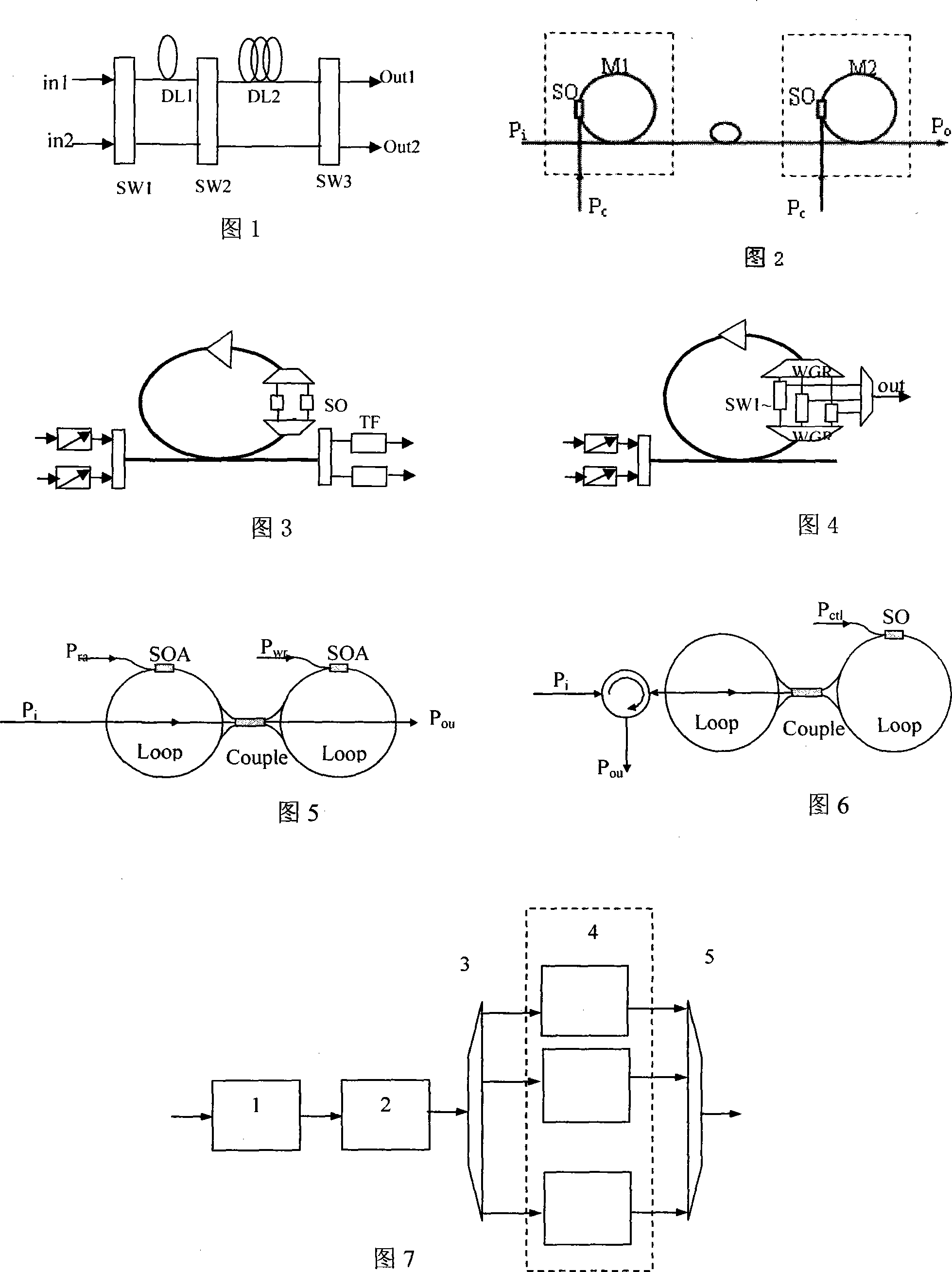
[0038] The double-loop coupled all-optical buffer, as shown in Figure 5 and Figure 6, not only stores optical signals, but also reads and writes under the control of another optical signal. This kind of buffer utilizes two sides ports of a 3×3 optical fiber coupler to form a double-ring structure through optical fiber feedback, and the middle port is used as the input and output ports of the buffer. It has two structures: through and return. The pass-through structure is shown in Figure 5. The middle ports on both sides of the 3×3 fiber coupler are used as the input and output ports respectively. There is an SOA in each fiber ring, and the control...

Embodiment 2

[0040] The power equalizer 1 and power equalizer 4 groups (they are composed of the same kind of devices) are erbium-doped fiber amplifiers, which have obvious gain saturation characteristics. Buffer unit 3 uses the buffer unit of "reflective optical fiber (FP cavity) + optical switch". The optical switch at both ends of the buffer uses a nonlinear loop mirror NOLM, or uses a T-bit asymmetric demultiplexer TOAD, or uses Nonlinear Fiber Sagnec Interferometer NFSI (Nonlinear Fiber Sagnec Interferometer) and other optical switches.

Embodiment 3

[0042] The power equalizer 1 and the power equalizer 4 groups (they are composed of the same device) are optical fiber Raman amplifiers, which have obvious gain saturation characteristics. The cache unit 3 uses a cache unit of "optical fiber ring + optical switch".


PUM


Abstract

The utility model relates to an all-optical buffer of multiple wavelength parallel storage to solve parallel buffer problem of dense wave-division multiplex signal and consists of an input power equalizer, a light buffer unit, a wave-division multiplex-de-multiplexer, an output power equalizer set and a wave-division multiplexer. The utility model adopts the multiple wavelength parallel storage technique of power equalization - parallel buffer - de-multiplex - power equalization - re-multiplex to maintain the synchronous buffering of multiple wavelength signals, so that the cross modulation among multiple wavelength signals can be effectively overcome, the signal-to-noise ratio can be promoted and the good buffer memory performance can be gained. Free adjustment on the cycle multiple of multiple wavelength signals buffer period can be realized in the utility model and the reading and writing time can be controlled with light signal writing and reading. The reading time can be started as required after storing signals; the event triggering can be realized without preset in the buffer. With great flexibility, the utility model is a real all-optical buffer suitable to all-optical routers or all-optical exchangers.

Description

technical field [0001] The invention relates to the technical field of optical communication, in particular to a multi-wavelength parallel buffer all-optical buffer, that is, an optical buffer for parallel buffering of multi-wavelength wavelength division multiplexing signals. Background technique [0002] With the development of high-speed all-optical networks, the shortcomings of wavelength switching are gradually emerging. All-optical networks are transitioning from optical wavelength switching networks with wavelength as the granularity of switching to optical packet switching networks with packet granularity. Optical packet switching will become an all-optical network. One of the important directions of the network. All-optical packet switching is essentially a store-and-forward technology, so how to complete the storage of optical data packets in the optical domain becomes the key technology of all-optical packet switching. The capacity, throughput, and packet loss ra...

Claims


Application Information

Patent Timeline
IPC IPC(8): H04B10/17H04L12/56H04J14/02G02B6/26H04B10/294
Inventor 吴重庆田昌勇彭鹏
Owner BEIJING JIAOTONG UNIV
Learn More