High-pressure resistant silicon carbide light guide switch

A high withstand voltage silicon carbide and photoconductive switch technology, which is applied in semiconductor devices, electrical components, circuits, etc., to achieve the effects of high withstand voltage structure, simple structure design, and improved compressive strength

Active Publication Date: 2008-02-27
SHANGHAI INST OF CERAMIC CHEM & TECH CHINESE ACAD OF SCI
View PDF0 Cites 25 Cited by
  • Summary
  • Abstract
  • Description
  • Claims
  • Application Information

AI Technical Summary

Problems solved by technology

However, due to the influence of light transmission efficiency, the withstand voltage of the switch is only 4000V

Method used


Image

  • High-pressure resistant silicon carbide light guide switch
  • High-pressure resistant silicon carbide light guide switch
  • High-pressure resistant silicon carbide light guide switch

Examples


Embodiment 1

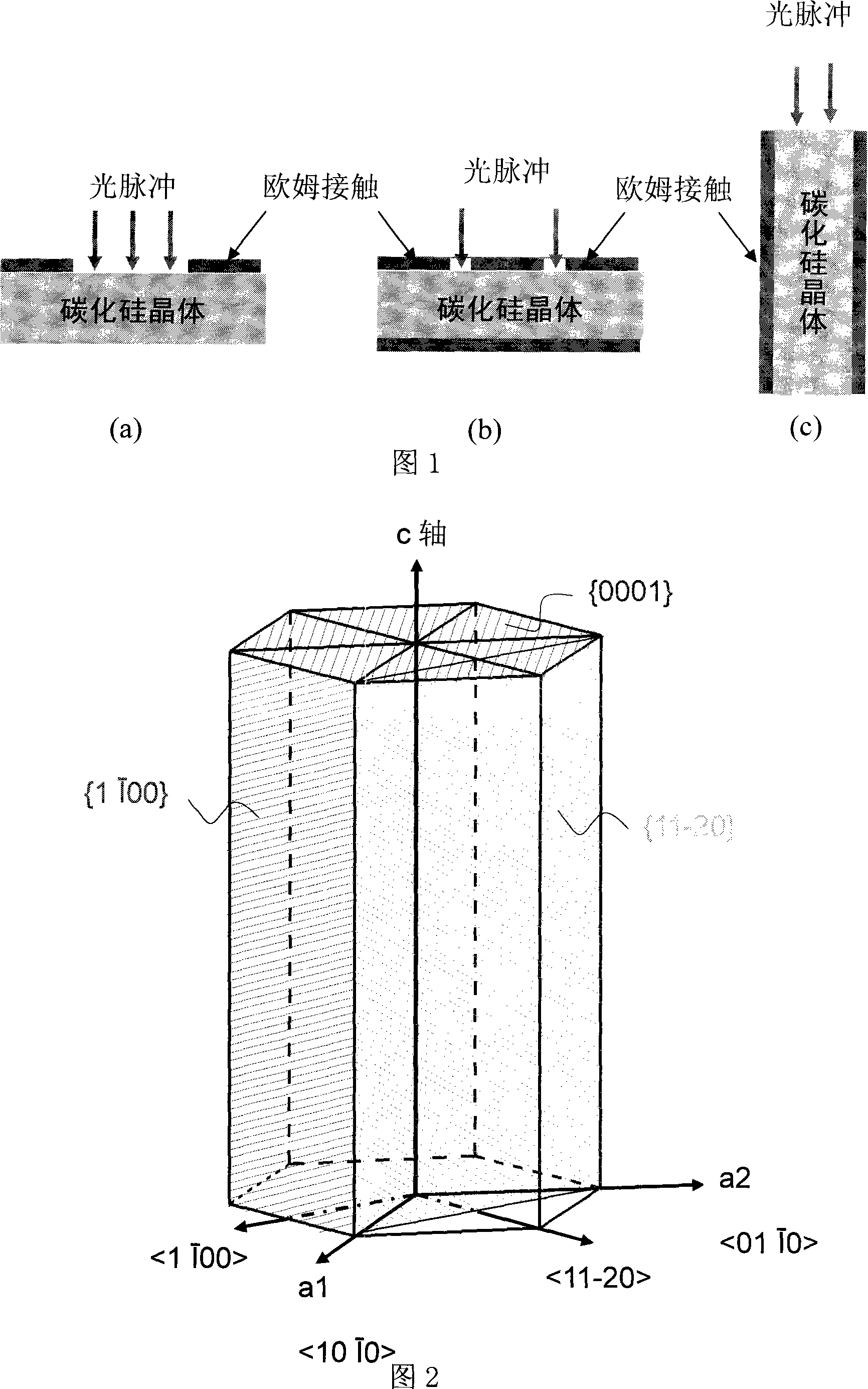
[0030] Opposite-plane photoconductive switch obtained by using (0001) plane semi-insulating SiC crystal.

[0031] The wafer used in the SiC photoconductive switch is a semi-insulating 6H-SiC crystal obtained by doping vanadium. The wafer sample is cut along the direction perpendicular to the c-axis of the crystal. The crystal plane is (0001). mm×10.0mm, the surface roughness Ra of the crystal detected by AFM is less than 0.5nm. In order to remove the surface oxide layer and the sub-damaged layer formed during processing, and passivate the wafer surface, the SiC wafer was annealed at 1000°C for 15 hours, then immersed in 200°C molten KOH solution for 3min etching, and finally Soak it in dilute HF for 12 hours, and then clean it according to the RCA process, so as to prepare for the production of device electrodes.

[0032] The device fabricated in the experiment adopts the opposite surface electrode structure, the electrode is square, the side length is 3.5mm, and the vertical...

Embodiment 2

[0035] Opposite-plane photoconductive switches obtained using (11-20) plane semi-insulating SiC crystals.

[0036] The wafer used in the SiC photoconductive switch is a semi-insulating 6H-SiC crystal obtained by doping vanadium. The wafer sample is cut along the direction parallel to the c-axis of the crystal. The crystal plane is (11-20), and the thickness after double-sided polishing is 0.5mm. It is 10.0mm×10.0mm, and the surface roughness Ra of the crystal detected by AFM is less than 0.5nm. In order to remove the surface oxide layer and the sub-damage layer formed during processing, and passivate the wafer surface, the SiC wafer was annealed at 1000°C for 15 hours, then immersed in 200°C molten KOH solution for 3min etching, and finally Soak it in dilute HF for 12 hours, and then clean it according to the RCA process, so as to prepare for the production of device electrodes.

[0037]The device fabricated in the experiment adopts the opposite surface electrode structure, a...


PUM


Abstract

The present invention relates to a high-pressure-resisted, silicon-carbide, photoconductive switch, and belongs to field of semiconductor device processing technology. The photoconductive switch takes relative-surface-shape design; the processed silicon-carbide polished wafer is form with ohmic contacts on its two surfaces, and the electrodes are formed. The relative-surface-shape, silicon-carbide, photoconductive switch can increase duplicate times of pressure resistance of the switch, and minimize volume of the photoconductive switch. The present invention creates conditions for integrating photoconductive switches, and can be used in field of semiconductor switches.

Description

technical field [0001] The invention relates to a high-voltage-resistant silicon carbide photoconductive switch, which belongs to the technical field of semiconductor device preparation. Background technique [0002] Photoconductive Semiconductor Switches (PCSS for short) is a semiconductor optoelectronic device that has developed rapidly in the past ten years. Its working principle is to use the photoelectric effect of the semiconductor material to modulate the resistivity of the material, that is, when the light is irradiated on the semiconductor material, the electrons in the valence band in the material absorb photon energy, jump into the conduction band through the forbidden band, and make the electron concentration in the conduction band and The increase of holes in the valence band will stimulate the photogenerated electron-hole pairs, which will make the semiconductor material produce electric effect. Photoconductive switches have extremely excellent characteristics...

Claims


Application Information

Patent Timeline
Patent Type & Authority Applications(China)
IPC IPC(8): H01L31/101H01L31/0224H01L31/036
Inventor 陈之战施尔畏严成锋肖兵
Owner SHANGHAI INST OF CERAMIC CHEM & TECH CHINESE ACAD OF SCI
Why Eureka
Try Eureka