

Strip preparation method of graphics ferroelectric lead zirconate titanate film
A lead zirconate titanate, ferroelectric thin film technology, applied in the manufacture of circuits, electrical components, semiconductor/solid-state devices, etc., to achieve the effect of improving compatibility, improving quality, and avoiding strong acid corrosive liquids
- Summary
- Abstract
- Description
- Claims
- Application Information
AI Technical Summary
Problems solved by technology
Method used
Image

Examples
Embodiment 1
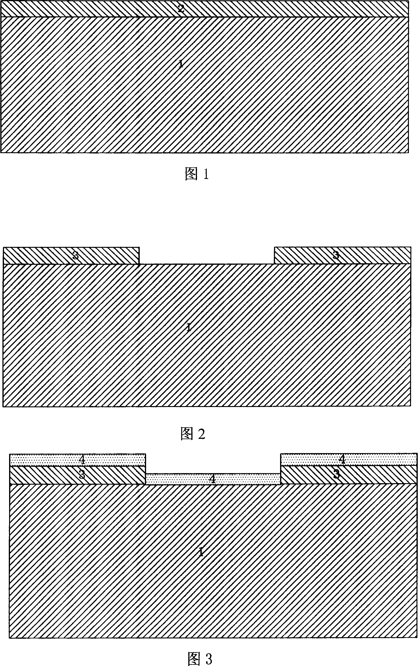
[0050] 1) Clean the silicon substrate
[0051] The silicon substrate 1 is first cleaned with an acidic cleaning solution or an alkaline cleaning solution, and then rinsed with deionized water;
[0052] 2) Preparation of zinc oxide sacrificial layer
[0053] Prepare a 0.01 μm zinc oxide sacrificial layer 2 on the cleaned substrate 1 by radio frequency sputtering equipment; coat a positive photoresist on the surface of the zinc oxide 2, and use the negative plate of the PZT film pattern to photoresist the positive photoresist Engraving exposure, using phosphoric acid as an etching solution to wet pattern the sacrificial layer 3;
[0054] 3) Preparation of PZT film guiding layer
[0055] Prepare a 0.01 μm PZT film guiding layer 4 on the patterned sacrificial layer 3 by using sputtering equipment, and the heating temperature of the substrate is 650°C;
[0056] 4) Preparation of PZT Pu membrane
[0057] A 0.01 μm PZT thin film 4 is prepared by sputtering equipment, and the heatin...
Embodiment 2
[0061] 1) Clean the potassium nitride substrate
[0062] The potassium nitride substrate 1 is first cleaned with an acid cleaning solution or an alkaline cleaning solution, and then rinsed with deionized water;
[0063] 2) Preparation of zinc oxide sacrificial layer
[0064] Prepare a 0.01 μm zinc oxide sacrificial layer 2 on the cleaned substrate 1 by radio frequency sputtering equipment; coat a positive photoresist on the surface of the zinc oxide 2, and use the negative plate of the PZT film pattern to photoresist the positive photoresist Engraving exposure, using phosphoric acid as an etching solution to wet pattern the sacrificial layer 3;
[0065] 3) Preparation of PZT film
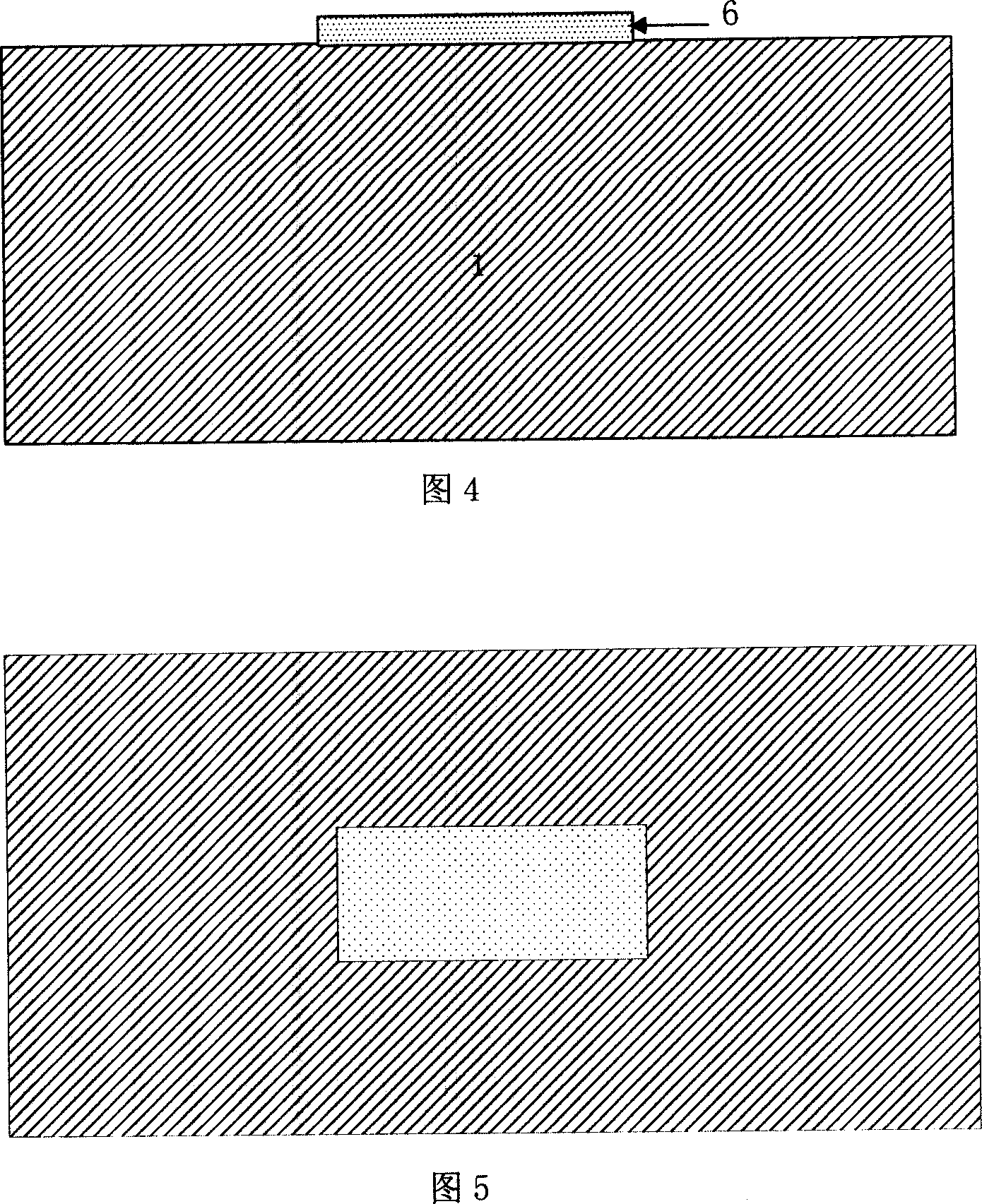
[0066] A 0.01 μm PZT thin film 4 is prepared by sputtering equipment, and the heating temperature of the substrate is 200° C.;
[0067] 4) Patterned PZT film
[0068] Put the substrate after the above process into the sodium hydroxide etching solution, release the sacrificial layer, and peel off...
Embodiment 3
[0070] 1) Clean the potassium arsenide substrate
[0071] The potassium arsenide substrate 1 is first cleaned with an acid cleaning solution or an alkaline cleaning solution, and then rinsed with deionized water;
[0072] 2) Preparation of zinc oxide sacrificial layer
[0073] Prepare a 5 μm zinc oxide sacrificial layer 2 on the cleaned substrate 1 by metal-organic decomposition method equipment; apply a negative photoresist on the surface of the zinc oxide sacrificial layer 2, and use a positive version of the PZT film pattern to negative photoresist Photolithographic exposure to form a sacrificial layer photoresist pattern; using phosphoric acid as an etching solution to wet-etch the patterned sacrificial layer 3;
[0074] 3) Preparation of PZT film
[0075] A 10 μm PZT thin film 4 is prepared by the sol-gel method, and the maximum heating temperature of the substrate is 800°C;
[0076] 4) Patterned PZT film
[0077] Put the substrate after the above process into the pho...
PUM
| Property | Measurement | Unit |
|---|---|---|
| Thickness | aaaaa | aaaaa |
| Thickness | aaaaa | aaaaa |
Abstract
Description
Claims
Application Information