Quantum dot material structure and its growth method

A technology of quantum dot material and growth method, which is applied in the field of positioning growth and process control of quantum dot materials with low-dimensional semiconductor structures, can solve the problems of unsatisfactory quantum dot position distribution control and affect the photoelectric performance of quantum dots, etc., and achieve simple process Effect

Inactive Publication Date: 2008-03-19
INST OF SEMICONDUCTORS - CHINESE ACAD OF SCI
View PDF0 Cites 13 Cited by
  • Summary
  • Abstract
  • Description
  • Claims
  • Application Information

AI Technical Summary

Problems solved by technology

Although this method avoids the pollution and defects caused by the substrate treatment before growth, the control of the position distribution of quantum dots by this method is not ideal.
In addition, the quantum dots positioned on the dislocation grid also affect the photoelectric performance of the quantum dots due to the short distance from the dislocations.

Method used


Image

  • Quantum dot material structure and its growth method
  • Quantum dot material structure and its growth method
  • Quantum dot material structure and its growth method

Examples


Embodiment

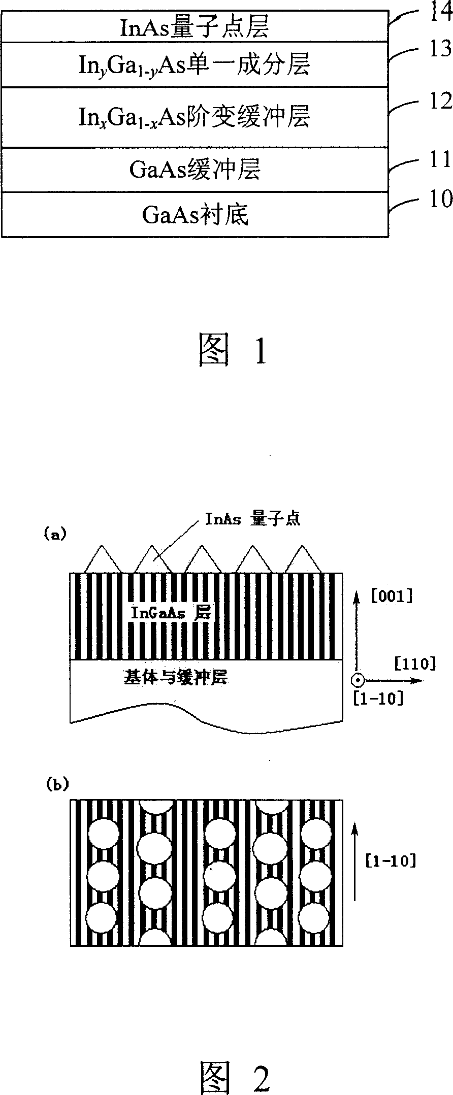
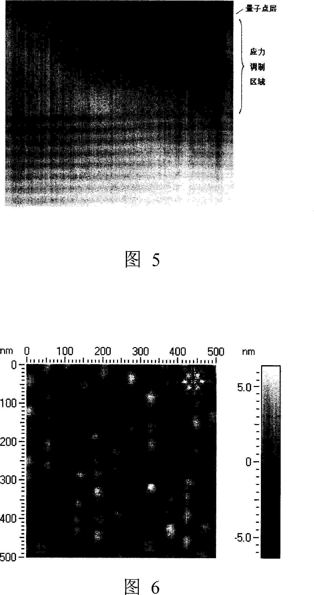
[0071] A 200nm thick GaAs buffer layer was grown on a GaAs (001) substrate with a 2° bias at 600°C, and then the substrate temperature was lowered to 400°C to grow an InGaAs step-change buffer layer. The step-change buffer layer has nine sub-layers, each with a thickness of 100 nm. The In composition changes from the first step's In0.03Ga0.97As to the ninth step's In at an increasing rate of 0.03. 0.27 Ga 0.73 As. Subsequent growth of In for 10 cycles 0.27 Ga 0.73 As(10nm) / In 0.27 Al 0.73 As (10nm) superlattice structure. Then the substrate temperature was increased to 450°C, and 200nm thick In 0.24 Ga 0.76 As layer. The substrate temperature is increased to 500℃, a 2.8ML thick InAs layer is deposited to form quantum dots, and then the temperature is reduced to 450℃ to grow 50nmIn 0.24 Ga 0.76 As spacer layer. The InAs quantum dots and spacer layer structure are repeatedly grown for three cycles, and finally the substrate becomes 500°C grown surface quantum dots with a thickness o...


PUM


Abstract

The invention discloses a quantum point material structure. The structure comprises a gallium arsenide GaAs substrate (10) for supporting the whole quantum point material structure, an epitaxial layer structure growing on the GaAs substrate (10) and comprising buffer layers (11,12,13) and an InAs quantum point layer (14), wherein the buffer layer comprises a GaAs buffer layer (11), an InxGa(1-x)As order variable buffer layer (12) and an InyGa(1-y)As single component layer (13) which grows in order on the substrate; and the InAs quantum point layer (14) grows on the InyGa(1-y)As single component layer (13). The invention further discloses a growth method of the quantum point material structure. With the inventive method, the large-area quantum points with ordered distribution are prepared by using the simple preparation process, the process is simple without special treatment of the substrate before growth and is completely compatible with the molecular beam epitaxy process. Additionally, the method is suitable for the bulk production of self-organization ordered-arrangement quantum point array material, which is significant for the quantum point material to be applied to the future quantum devices.

Description

Technical field [0001] The invention relates to the technical field of low-dimensional semiconductor structure quantum dot material positioning growth and process control, in particular to a quantum dot material structure that is positioned and grown by in-situ technology and a growth method thereof. Background technique [0002] Due to their unique electronic structure and density of states, semiconductor quantum dot low-dimensional nanostructured materials exhibit excellent optoelectronic properties, and have very important application prospects in the fields of nanoelectronics and photonics in the future. The theory predicts that quantum dot lasers have better performance than quantum well lasers in many aspects, such as higher gain, lower threshold current, higher quantum efficiency and better thermal stability. In addition, by using the "tunneling" effect of electrons in quantum dots, the number of electrons entering or leaving the quantum dot can be precisely controlled to ...

Claims


Application Information

Patent Timeline
Patent Type & Authority Applications(China)
IPC IPC(8): H01L33/00H01L31/0304H01L31/18H01L21/20H01S5/00H01L33/12
CPCY02P70/50
Inventor 焦玉恒吴巨徐波金鹏王占国
Owner INST OF SEMICONDUCTORS - CHINESE ACAD OF SCI
Why Eureka
Try Eureka