Method for improving luminance brightness of chip at the axial direction

An axial, photometric technology, applied in electrical components, circuits, semiconductor devices, etc., to solve problems such as limiting photons

Inactive Publication Date: 2008-04-16
HANGZHOU SILAN AZURE
View PDF0 Cites 7 Cited by
  • Summary
  • Abstract
  • Description
  • Claims
  • Application Information

AI Technical Summary

Problems solved by technology

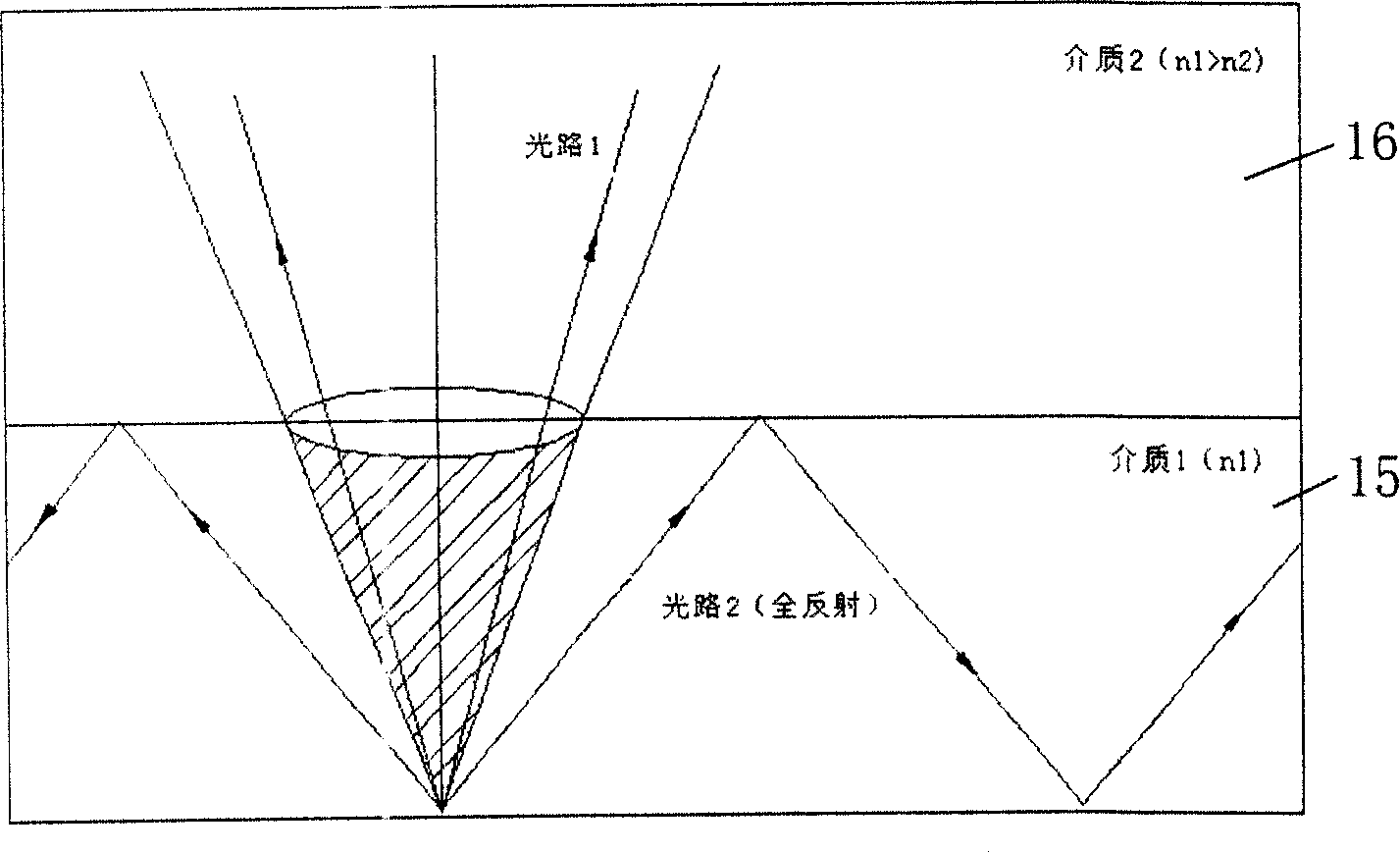
[0003] At present, although the electro-optic conversion efficiency can reach more than 75%, the total reflection phenomenon will occur at the interface when the light is incident from the high-refractive-index medium to the low-refractive-index medium, which greatly limits the probability of photons escaping the luminescent medium.
like image 3 As shown, light enters the medium 16 of low refra

Method used


Image

  • Method for improving luminance brightness of chip at the axial direction
  • Method for improving luminance brightness of chip at the axial direction
  • Method for improving luminance brightness of chip at the axial direction

Examples


Embodiment Construction

[0014] Please see attached Figure 4 Shown in (a) to (e), the present invention will be further described below in conjunction with the accompanying drawings and embodiments.

[0015] first reference Figure 4 (a), depositing a layer of nickel (Ni) metal 42 with a thickness between 1 and 50 nanometers on the surface of the sapphire substrate 41;

[0016] followed by Figure 4 (b), perform rapid annealing at a temperature of 600-900 degrees Celsius for 30-300 seconds, at this time, the nickel metal 42 will form a small ball with a diameter of about 200-400 nanometers, which is used as a mask;

[0017] exist Figure 4 In (c), use an inductively coupled reactive ion etcher (ICP-RIE) to selectively etch the surface of the sapphire substrate with reactive gases (such as chlorine, boron trichloride, and methane) to achieve surface roughening , the etching depth is generally around 100~500nm

[0018] Figure 4 (d), nickel metal 42 is etched clean with chemical solution;

[001...


PUM


Abstract

The present invention discloses a method for improving axial brightness of chip, and is characterized in that the method further comprises the following procedures: step 1, a layer of nickel metal with the thickness between 1 nanometer and 50 nanometer is coated on the surface of a sapphire substrate by vapor deposition; step 2: the nickel metal is rapidly annealed for 30 seconds to 300 seconds with the temperature of 600 DEG C to 900 DEG C, then the nickel metal forms a globular shape with the diameter between 200 nanometers and 400 nanometers, and is used as a mask; step 3, the surface of the sapphire substrate is etched selectively and the depth is between 100 nanometers and 500 nanometers; step 4, the nickel metal on the sapphire substrate is cleaned; step 5, indium gallium nitride epitaxial layer grows from the sapphire substrate. The technical proposal of the invention can reduce the full reflection of emergent light and improve axial brightness.

Description

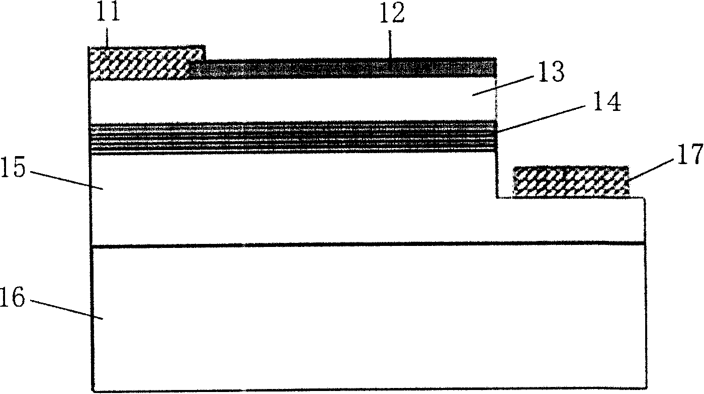
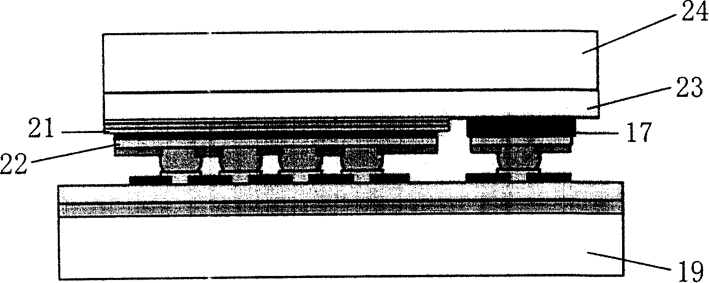
technical field [0001] The invention relates to a method for improving the axial luminance of a chip, in particular to a method for forming a nanoscale roughened structure at the interface between a chip substrate and an epitaxial layer. Background technique [0002] The general blue-green light-emitting diode LED is made by epitaxially growing an indium gallium nitride single crystal material structure on a smooth and flat sapphire substrate, and realizing (N) negative type and (P) positive type by adding silicon and magnesium elements respectively. Semiconductor materials, and adjust the wavelength of light emission by adjusting the ratio of indium gallium in the active layer. After the epitaxial process, it needs to go through photolithography and cleaning of the chip surface, electrode production, etching of the negative electrode area, detection of light emission characteristics, Thinned and cut into discrete chips, so a traditional blue-green chip structure is as figu...

Claims


Application Information

Patent Timeline
IPC IPC(8): H01L33/00
Inventor 陈立人
Owner HANGZHOU SILAN AZURE
Why Eureka
Try Eureka