Nanocrystalline porous TiO2 film and preparation method thereof
A nanocrystalline and thin-film technology, applied in chemical instruments and methods, gaseous chemical plating, coating, etc., can solve environmental pollution and other problems, and achieve the effects of simple equipment, less pollution, and low cost
- Summary
- Abstract
- Description
- Claims
- Application Information
AI Technical Summary
Problems solved by technology
Method used
Image
Examples
Embodiment 1
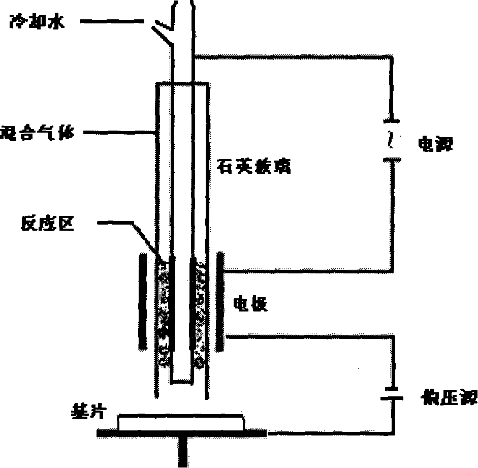
[0033] use figure 1 The plasma reactor shown. Under normal temperature and pressure, two coaxial quartz glass tubes with a thickness of 2mm are used as the blocking medium, aluminum foil electrodes, the electrode thickness is 0.2mm, the electrode spacing is 8mm, and the power supply is 1000W. The bias voltage is 300v, and the pulse ratio is 0.18.
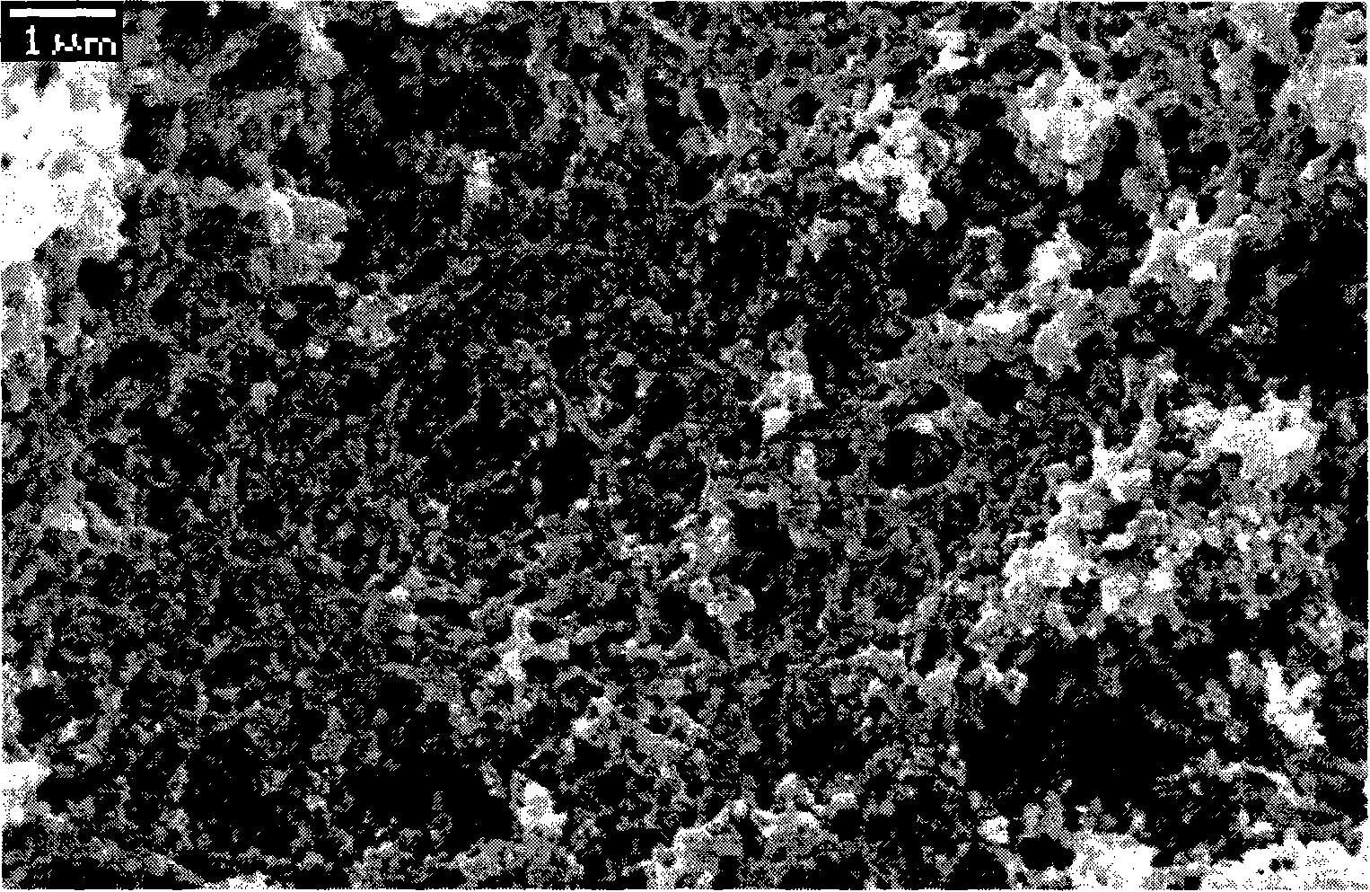
[0034] Ultrasonic clean the ordinary glass slide, place it at 0.5mm below the reactor, and now pass pure Ar (1SLM) for 5 minutes, and then pass O2 and the mixed gas of the monomer brought in by Ar, the mixing ratio is TiCl4: O2:Ar=1:5:100, flow rate 1SLM, take out the sample after discharge for 3 minutes, observe with scanning electron microscope, it is crystal structure with porous structure, grain size is 100-500nm, pore size is 20-5000nm. SEM as figure 2 shown.
Embodiment 2
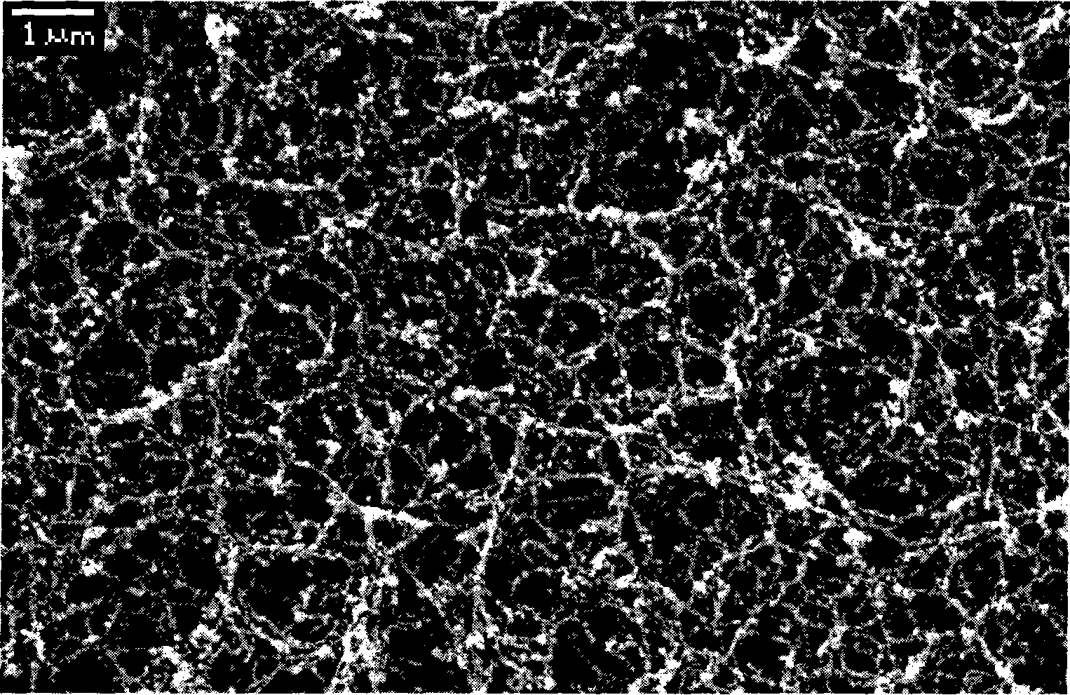
[0036] use figure 1 The plasma reactor shown. Under normal temperature and pressure, a coaxial alumina ceramic tube with a thickness of 3mm is used as the blocking medium, an aluminum foil electrode, the electrode thickness is 0.2mm, the electrode spacing is 10mm, and the power supply is 2000W. Bias - 600V. Ultrasonic clean the silicon wafer, place it 5mm below the reactor, pass pure Ar (1SLM) for 5 minutes, and then pass O2 and the mixed gas of TEOS monomer brought in by Ar, the mixing ratio is TEOS:O2: Ar=1:50:300, the flow rate is 5SLM, the sample is taken out after 10 minutes of discharge, and observed by a scanning electron microscope, it is a porous crystal structure with a grain size of 20-200nm and a pore size of 20-3000nm. SEM as image 3 shown.
Embodiment 3
[0038] use figure 1 The plasma reactor shown. Under normal temperature and pressure, two layers of coaxial quartz glass tubes with a thickness of 2mm are used as the barrier medium, aluminum foil electrodes, the electrode thickness is 0.2mm, the electrode distance is 5mm, and the power supply is 500W. Bias -200V.
[0039] Ultrasonic clean the quartz plate, place it 1mm below the reactor, pass pure He (1SLM) into it for 5 minutes, then pass into the mixed gas of O2 and TiCl4 monomer brought in by He, the mixing ratio is TiCl4:O2: Ar=1:10:500, flow rate 0.5SLM, the sample was taken out after 15 minutes of discharge, observed under a polarizing microscope, and a bright crystal grain structure was displayed under polarized light. Polarizing microscope such as Figure 4 shown.
PUM
| Property | Measurement | Unit |
|---|---|---|
| Thickness | aaaaa | aaaaa |
Abstract
Description
Claims
Application Information


