Multilayer soft printed wiring board and production method thereof
A flexible printing and manufacturing method technology, which is applied in multilayer circuit manufacturing, printed circuit manufacturing, printed circuit, etc., can solve the problem that insulating resin cannot meet the requirements of thinning printed wiring boards, and reduce electrostatic capacitance and delay , to achieve the effect of thin film
- Summary
- Abstract
- Description
- Claims
- Application Information
AI Technical Summary
Problems solved by technology
Method used
Image

Examples
Embodiment 1
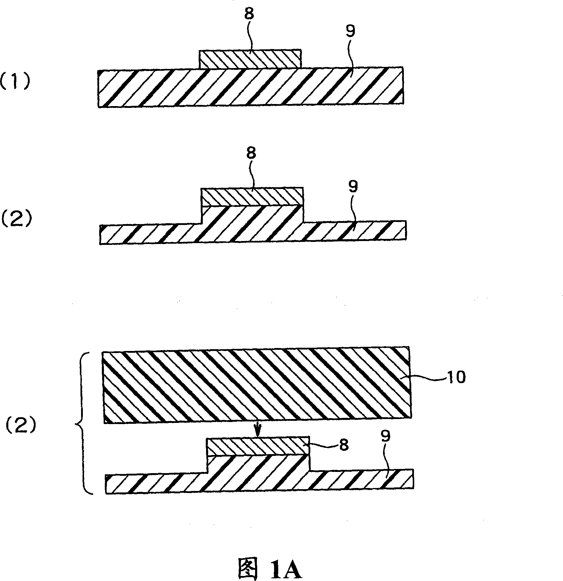
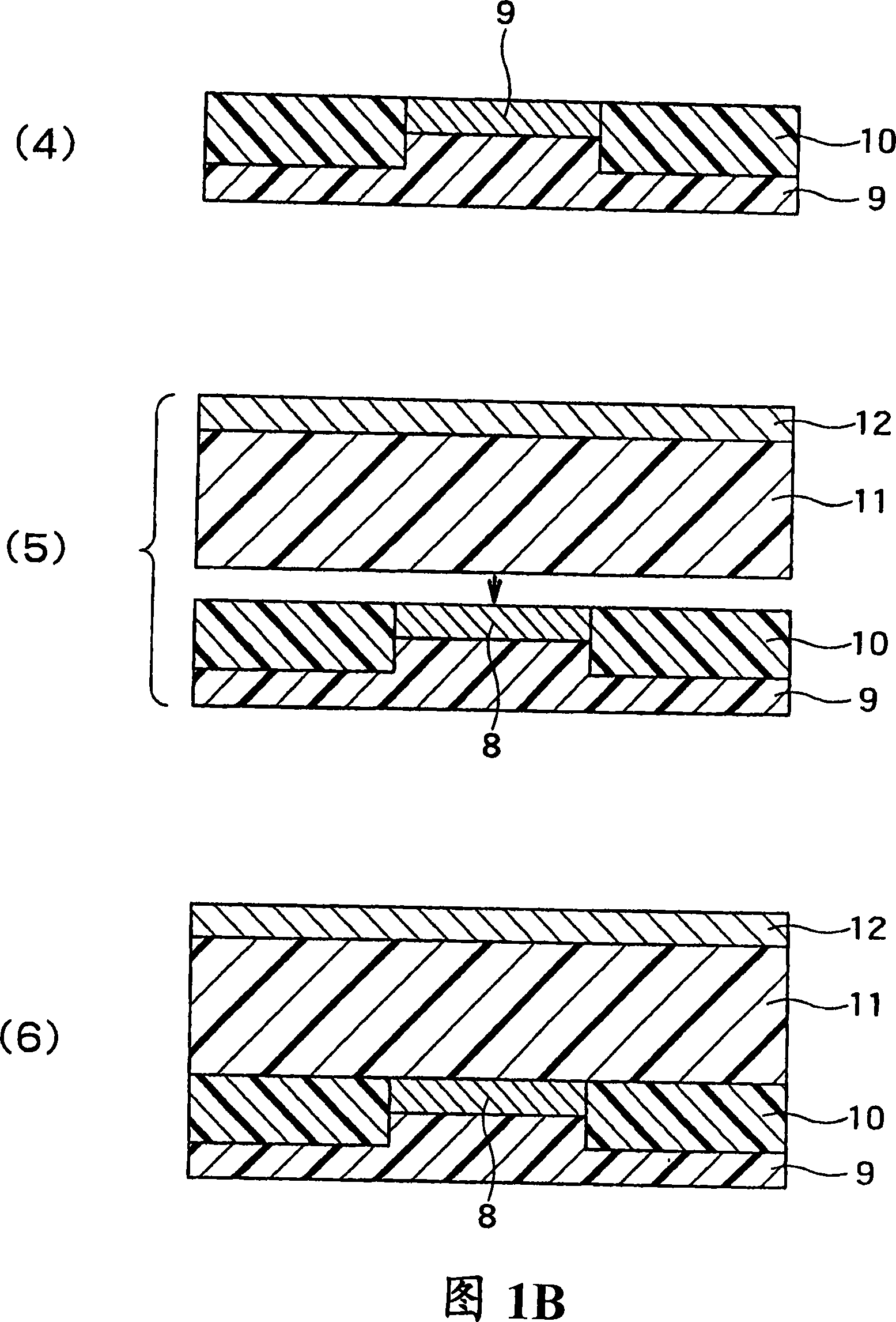
1A and 1B show the steps of Embodiment 1 of the present invention. First, as shown in FIG. 1A(1), wiring constituting the signal line 8 is formed on the first insulating layer 9 with a thickness of 25 μm by etching a copper foil with a thickness of 12 μm.
[0030]
In order to form this structure, the starting material is NeoflexNEX-23FE (25T) (Mitsui Chemical Co., Ltd.).
[0031]
Next, as shown in FIG. 1A(2), the first insulating layer 9 was removed to a thickness of 12.5 μm by chemical etching using an etchant TPE-3000 (manufactured by Toray Engineering Co., Ltd.) using the signal line 8 as a mask.
[0032]
Next, as shown in FIG. 1A (3), as the second insulating layer 10 with a low dielectric constant, Vexta (manufactured by KURARAY Co., Ltd., heat distortion temperature 275° C., dielectric constant 2.95 ) at a temperature higher than the heat distortion temperature of the liquid crystal polymer, and press and form it with a vacuum flat press.
[0033]
Thereafter, a...
Embodiment 2
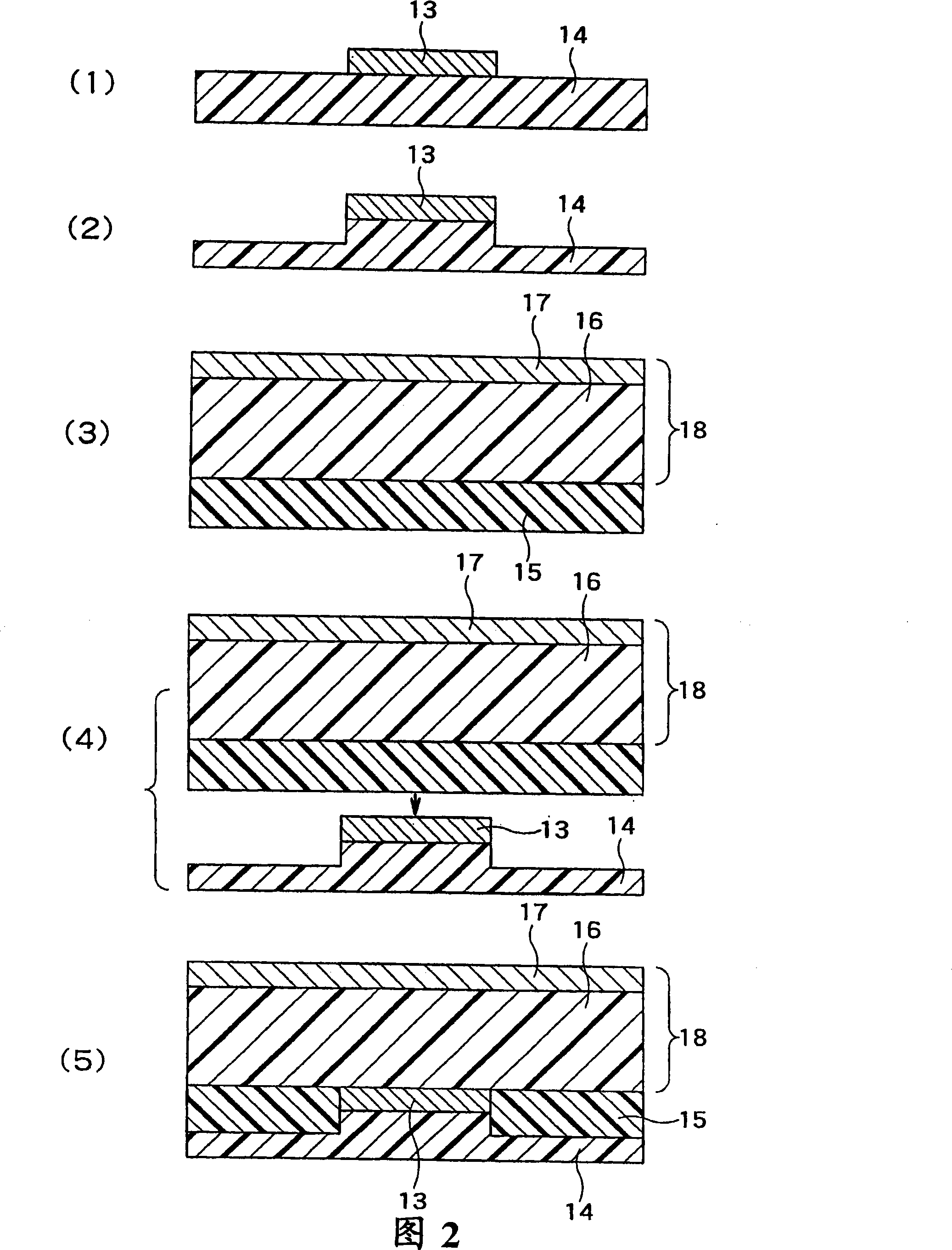
Fig. 2 shows the process of the second embodiment of the present invention. First, as shown in FIG. 2(1), wiring constituting the signal line 13 was formed on the first insulating layer 14 with a thickness of 25 μm by etching a copper foil with a thickness of 12 μm.
[0037]
In order to form this structure, the starting material used is NeoflexNEX-23FE (25T) (Mitsui Chemicals Co., Ltd. Co., Ltd.).
[0038]
Next, as shown in FIG. 2(2), the first insulating layer 14 was removed to a thickness of 13 μm by chemical etching using an etchant TPE-3000 (manufactured by Toray Engineering Co., Ltd.) using the signal line 13 as a mask.
[0039]
Next, as shown in FIG. 2(3), Vexta (manufactured by KURARAY Co., Ltd., heat distortion temperature 240° C., dielectric constant 2.95) which is a liquid crystal polymer with a thickness of 25 μm as the second insulating layer 15 with a low dielectric constant and a liquid crystal polymer single-sided copper-clad laminate Espanex LC-12-50-00N...
Embodiment 3
3A and 3B show the steps of the third embodiment of the present invention. First, as shown in FIG. 3A (1), by etching copper foil with a thickness of 12 μm, the wiring constituting the signal line 19 is formed on the first insulating layer 20 having a copper foil of 12 μm and a thickness of 25 μm constituting the first planar layer 21. superior.
[0043]
In order to form the structure of the third embodiment, the starting material is a single polyimide that integrates the first insulating layer 20, the signal line 19 and the copper foil constituting the first plane layer 21, and can be chemically etched homogeneously. Metaroyal (manufactured by Toyo Metal Spray Co., Ltd.) PI-25D-CCW-12D0 (#25) composed of Kapton EN layer.
[0044]
Next, as shown in FIG. 3A (2), use a chemical etching method, use the signal line 19 as a mask, etchant TPE-3000 (manufactured by Toray Engineering Co., Ltd.) to etch the first insulating layer 20 to the first plane layer 21 surfaces.
Next, as...
PUM
 Abstract
Description
Claims
Application Information
 - R&D
- Intellectual Property
- Life Sciences
- Materials
- Tech Scout
- Unparalleled Data Quality
- Higher Quality Content
- 60% Fewer Hallucinations
Browse by: Latest US Patents, China's latest patents, Technical Efficacy Thesaurus, Application Domain, Technology Topic, Popular Technical Reports.
© 2025 PatSnap. All rights reserved.Legal|Privacy policy|Modern Slavery Act Transparency Statement|Sitemap|About US| Contact US: help@patsnap.com