Sub-mount and its manufacturing method

A manufacturing method and sub-mount technology, which can be used in manufacturing tools, semiconductor/solid-state device manufacturing, welding equipment, etc., and can solve the problems of increased substrate surface roughness, increased cost, and roughened electrode layer surface roughness.

Inactive Publication Date: 2008-06-04
DOWA ELECTRONICS MATERIALS CO LTD
View PDF5 Cites 14 Cited by
  • Summary
  • Abstract
  • Description
  • Claims
  • Application Information

AI Technical Summary

Problems solved by technology

In the case of using an adhesive layer of noble metal, there is a big problem of cost increase
[0031] In the case of forming electrodes on the submount by the lift-off method, the roughness of the substrate surface tends to increase, which ha...

Method used


Image

  • Sub-mount and its manufacturing method
  • Sub-mount and its manufacturing method
  • Sub-mount and its manufacturing method

Examples


Embodiment 1

[0156] Hereinafter, the present invention will be explained in more detail based on examples.

[0157] First, the manufacturing method of the submount will be described.

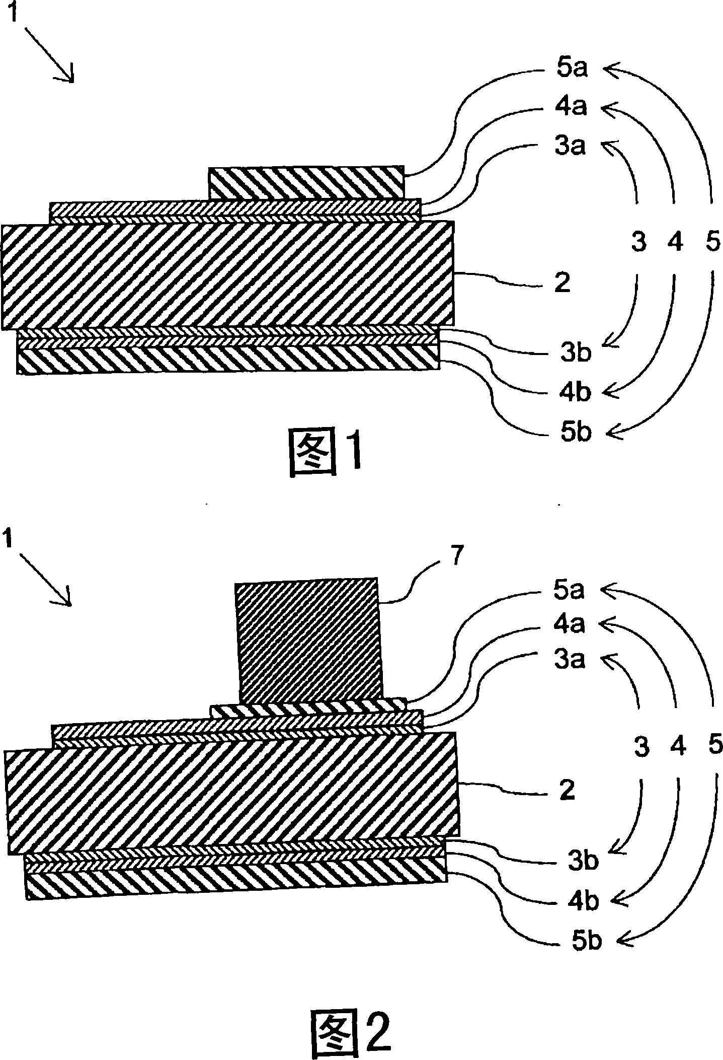
[0158] Both sides of a 55mm square and 0.3mm thick sintered aluminum nitride substrate 2 with high thermal conductivity (230W / mK) are ground by a polishing device, and the polishing device is used for finishing polishing to make the aluminum nitride substrate 2 rough The degree (Ra) is 0.07 μm.

[0159] The polished aluminum nitride substrate 2 is cleaned to clean the surface, and the substrate protective layer 3a made of titanium is deposited to a thickness of 0.05 μm on the entire surface of the substrate 2 by a vacuum vapor deposition device.

[0160] Next, in order to perform photolithographic layout, the entire surface of the substrate on which the substrate protective layer 3a has been deposited is uniformly coated with a resist using a spin coater, and then a predetermined baking is performed in a baking ...

Embodiment 2

[0165] The submount 1 of Example 2 was manufactured in the same manner as Example 1, except that the average roughness (Ra) of the aluminum nitride substrate 2 was 0.04 μm.

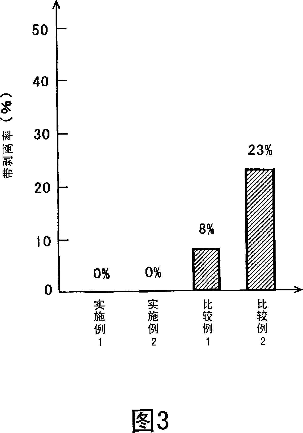
[0166] Next, a comparative example will be described.

Embodiment 3

[0195] Hereinafter, the present invention will be explained in more detail based on Examples 3 and 4. First, the manufacturing method of the submount of the third embodiment will be described.

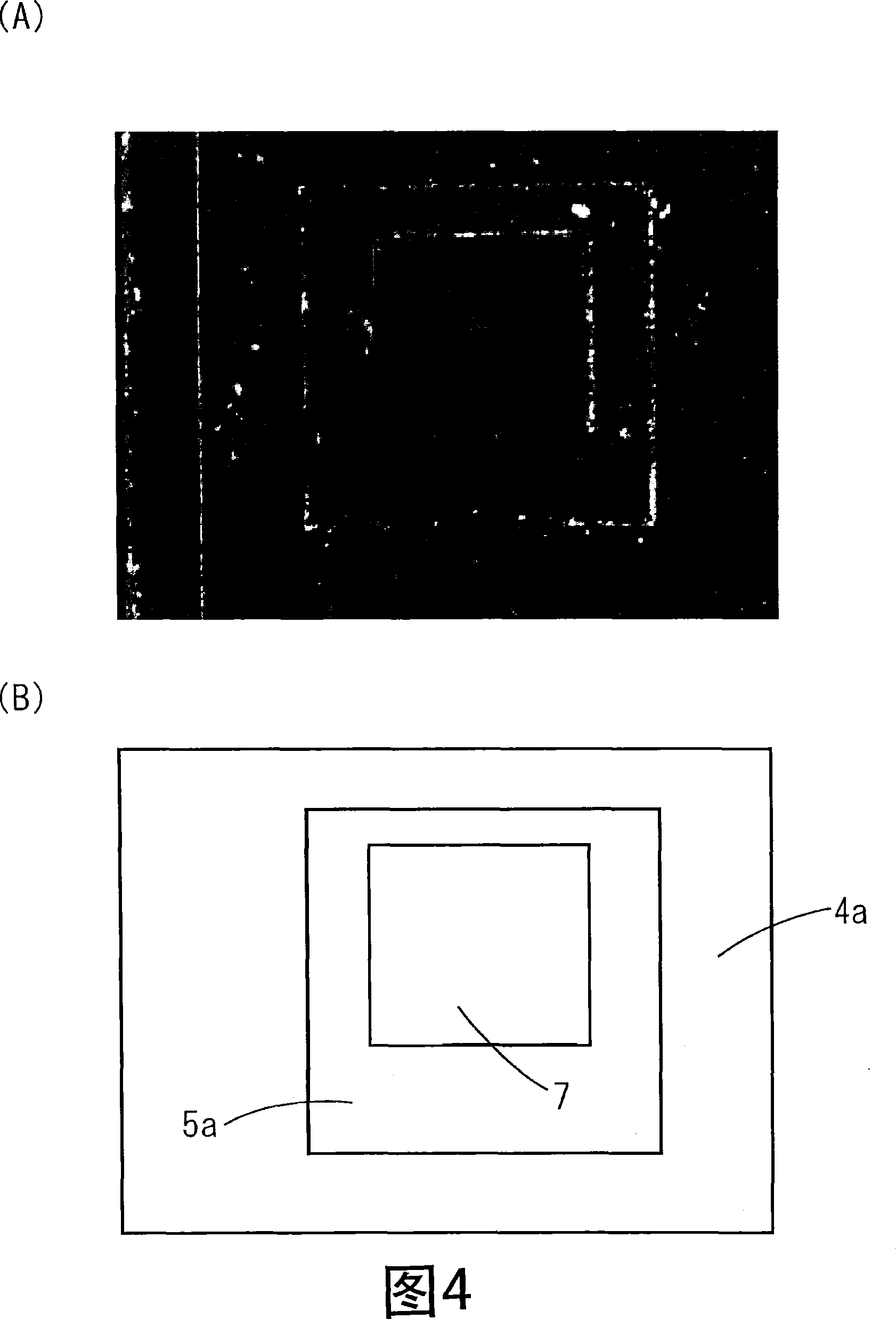
[0196] Grind both sides of a high thermal conductivity (230W / mK) aluminum nitride sintered substrate (55mm square, 0.3mm thick) with a polishing device. In addition, finishing grinding is performed using a polishing device. The polished aluminum nitride sintered substrate 12 is cleaned to clean the surface. In order to perform photolithographic patterning, a spin coater is used to uniformly coat the entire surface of the submount substrate 12 with a resist. A baking oven is used for predetermined baking, and a mask alignment device is used for gamma line contact exposure. The exposure mask is designed to be able to lay out 2500 at the same time with the submount size of 1mm square. After the exposure, the resist of the electrode layer is dissolved with a developer to expose the submount su...


PUM

PropertyMeasurementUnit
Average roughnessaaaaaaaaaa
Surface average roughnessaaaaaaaaaa

Abstract

A submount with an electrode layer having excellent wettability in soldering and method of manufacturing the same are disclosed. A submount (1) for having a semiconductor device mounted thereon comprises a submount substrate (2), a substrate protective layer (3) formed on a surface of the submount substrate (2), an electrode layer (4) formed on the substrate protective layer (3) and a solder layer (5) formed on the electrode layer (3) wherein the electrode layer (4) is made having an average surface roughness of less than 1 [mu]m. The reduced average surface roughness of the electrode layer (4) improves wettability of the solder layer (5), allowing the solder layer (5) and a semiconductor device to be firmly bonded together without any flux therebetween. A submount (1) is thus obtained which with the semiconductor device mounted thereon is reduced in heat resistance, reducing its temperature rise and improving its performance and service life.

Description

Technical field [0001] The present invention relates to a submount used in a semiconductor device and a manufacturing method thereof. Background technique [0002] Generally, when a semiconductor device is packaged, it is mounted on a heat sink or a heat sink to dissipate heat generated from the semiconductor device. In order to improve the heat dissipation characteristics, a substrate with high thermal conductivity, that is, a submount component, may be interposed between the semiconductor device and the heat dissipation plate. As the substrate with high thermal conductivity, aluminum nitride (AlN) and the like are known. [0003] In the case of joining the submount and the semiconductor device, the joining strength is required as one. In the prior art, the adhesion layer is provided by expensive noble metal, or the surface roughness of the substrate itself is adjusted in order to increase the bonding strength between the electrode layer arranged on the bottom surface of the bra...

Claims


Application Information

Patent Timeline
IPC IPC(8): H01L23/12H01L21/52B23K35/30
CPCH01L2924/0103H01L2924/01029H01L2924/01074H01L2924/0105H01L2924/01078H01L2924/01042H01L2924/01028H01L2924/01079H01L2924/01049H01L2924/014H01L2924/01013H01L2224/32225H01L2924/1301
Inventor 大鹿嘉和中野雅之
Owner DOWA ELECTRONICS MATERIALS CO LTD
Why Eureka
Try Eureka