System and method for controlling horizontally and focusing automatically silicon slice platform of photo-etching machine

An automatic focus and level control technology, which is applied in the direction of microlithography exposure equipment, optics, pattern surface photoplate making process, etc., can solve the problems that affect the detection accuracy, large focus depth, interference, etc., to improve detection accuracy and improve The effect of manufacturing process and equipment cost reduction

Inactive Publication Date: 2008-06-18
SHANGHAI HUA HONG NEC ELECTRONICS
View PDF0 Cites 8 Cited by
  • Summary
  • Abstract
  • Description
  • Claims
  • Application Information

AI Technical Summary

Problems solved by technology

This technique is simple and easy, but there are several problems: 1. The light source used to detect the horizontal position of the silicon wafer and the exposure light source are not coaxial, which restricts the accuracy of level control
2. Due to the long wavelength of the light source used and the large depth of focus, it is often easily disturbed by the substrate pattern, and the real surface of the silicon wafer cannot be detected, which affects the detection accuracy

Method used


Image

  • System and method for controlling horizontally and focusing automatically silicon slice platform of photo-etching machine
  • System and method for controlling horizontally and focusing automatically silicon slice platform of photo-etching machine
  • System and method for controlling horizontally and focusing automatically silicon slice platform of photo-etching machine

Examples


Embodiment Construction

[0010] The present invention will be further described in detail below in conjunction with the drawings and specific embodiments.

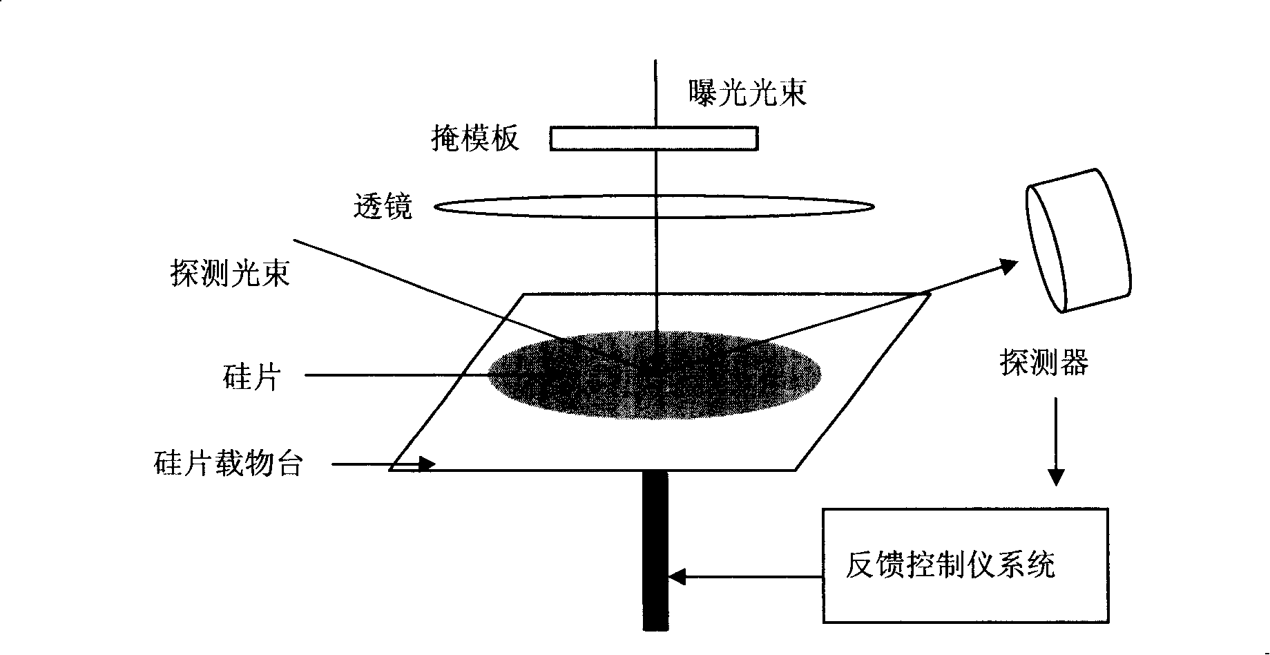
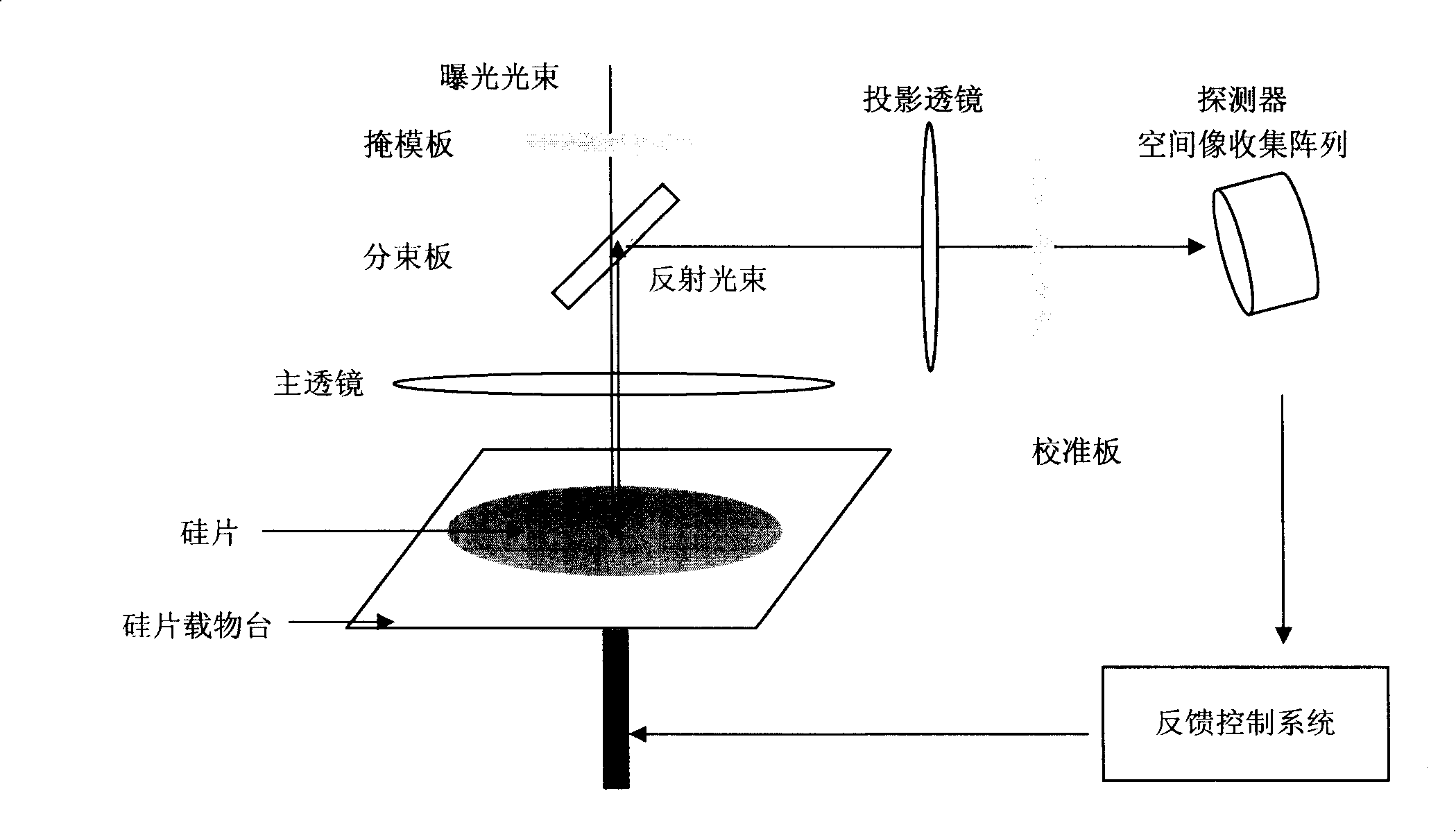
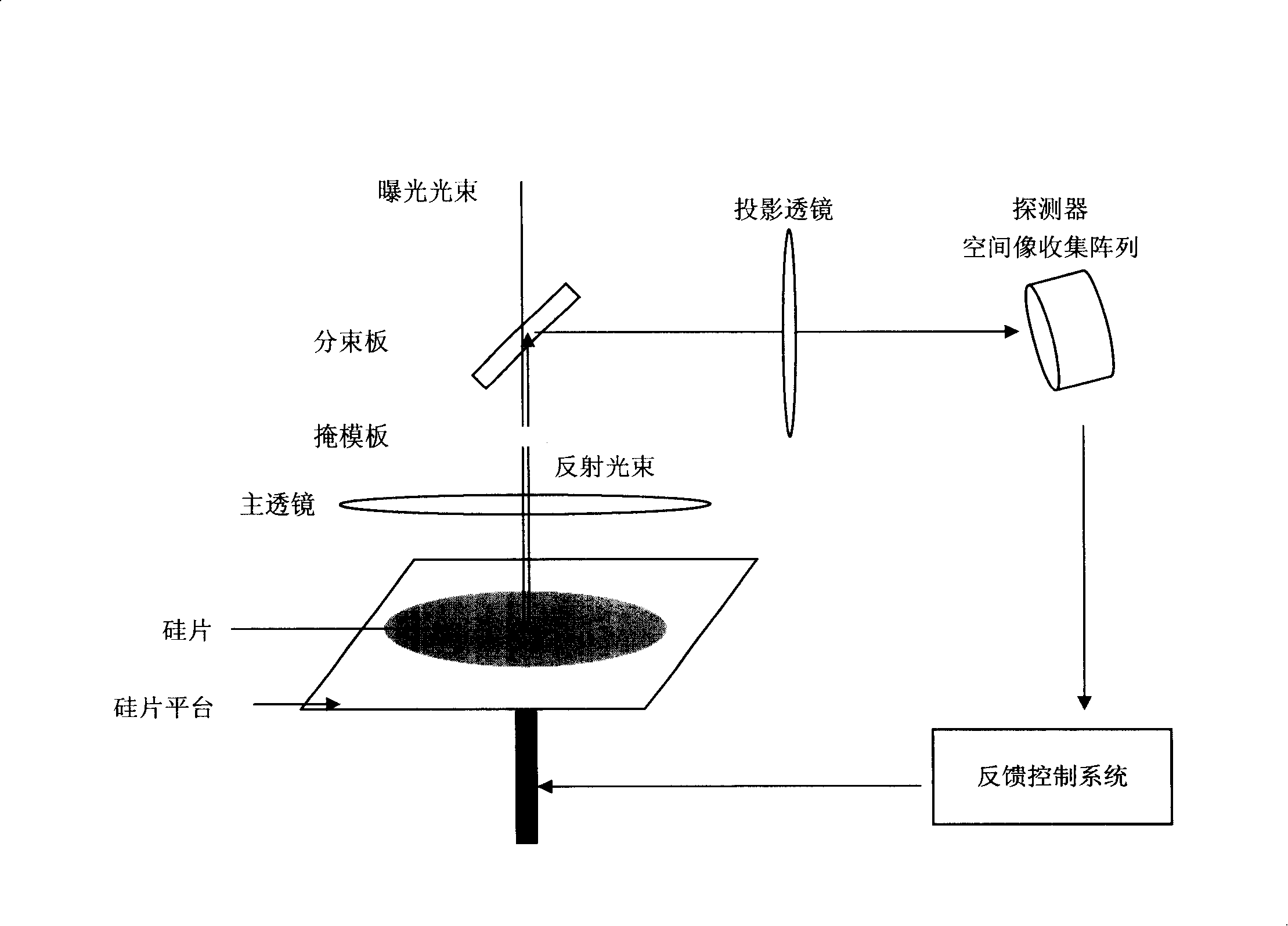
[0011] The invention is a silicon chip level control system of a photoetching machine used in projection photoetching for semiconductor integrated circuit printing, which uses the reflected beam of the exposure beam to confocal detection of the silicon chip position and real-time feedback control. As mentioned before (see figure 1 ), the silicon wafer stage control system in the prior art includes a mask, a lens, a silicon wafer stage, a focal plane spatial image collection detector array and a feedback controller system, etc. The feedback controller system can control the silicon The slide stage performs real-time feedback adjustment to automatically adjust the horizontal position of the silicon wafer and auto-focus; on this basis, the system of the present invention adds a projection lens and a beam splitting plate, the beam splitting plate can spl...


PUM


Abstract

The invention discloses a horizontal control and automatic focusing system for a silicon chip platform of a photoetching machine and a method thereof. The system comprises a mask plate, a lens, a silicon chip object stage, a focal plane space image collection detector array and a feedback controller system, moreover, the system also comprises a projection lens and a beam splitting plate which can conduct light splitting on the reflected light beam; the projection lens and the focal plane space image collection detector array collect the image formed by reflection on the surface of the silicon chip and amplify the image. According to the principle of reversibility of optical path, as the invention adopts the confocal detecting method usually used in optics, the invention improves detecting accuracy of the silicon chip horizontal control system and realizes automatic focusing, therefore, the invention improves the accuracy of the silicon chip horizontal control system and enlarges the photoetching technique window, moreover, the invention greatly decreases the requirement of the photoetching technology for the photoetching equipment while the cost of the equipment is reduced and manufacturing technique is improved; the invention can conduct horizontal position control and automatic focusing on the silicon chip in real time, accurately and automatically.

Description

Technical field [0001] The invention relates to a projection photoetching equipment in semiconductor manufacturing, in particular to a photoetching machine silicon wafer platform level control and automatic focusing system and method. Background technique [0002] At present, with the development of semiconductor technology and the progress of processing and manufacturing technology, the critical dimension (CD Critical Demotion) of semiconductor devices is getting smaller and smaller, and the difficulty of processing and manufacturing is also increasing. In the existing semiconductor manufacturing process, the semiconductor device mainly transfers the design pattern to various thin films grown on the surface of the silicon wafer through photolithography, and then forms the pattern through various etching methods. Among them, the photolithography technology directly determines the minimum critical dimensions that can be achieved by semiconductor devices in actual manufacturing. In...

Claims


Application Information

Patent Timeline
Patent Type & Authority Applications(China)
IPC IPC(8): G03F9/02G03F9/00G03F7/20
Inventor 王雷伍强
Owner SHANGHAI HUA HONG NEC ELECTRONICS
Why Eureka
Try Eureka