Method for production of silicon carbide layer, gallium nitride semiconductor device and silicon substrate

A silicon carbide layer and silicon substrate technology, which is applied in semiconductor/solid-state device manufacturing, electrical components, circuits, etc., can solve the problems of inability to form a group III nitride semiconductor layer and a non-silicon carbide layer, and achieve excellent crystallinity, The effect of suppressing ionization and preventing deterioration of crystallinity

Inactive Publication Date: 2008-06-18
SHOWA DENKO KK
View PDF1 Cites 3 Cited by
  • Summary
  • Abstract
  • Description
  • Claims
  • Application Information

AI Technical Summary

Problems solved by technology

However, according to the prior art, as described above, it is impossible to reliably form a silicon carbide layer uniformly covering the entire surface of a silicon substrate.
For this reason, when it is intended to form a GaN layer using a s...

Method used


Image

  • Method for production of silicon carbide layer, gallium nitride semiconductor device and silicon substrate

Examples


Embodiment Construction

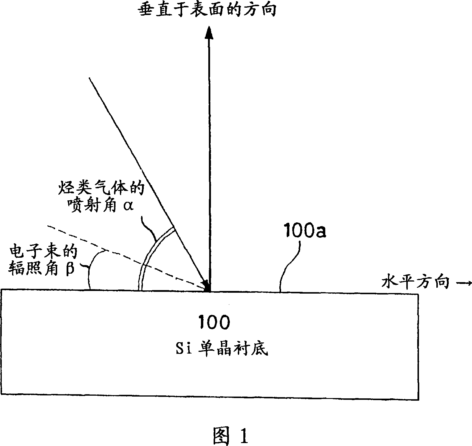
[0021] Cubic silicon carbide crystalline layers, in particular 3C-silicon carbide layers (SiC layers) according to the Ramsdell notation, can be formed as silicon substrates having surfaces with different crystallographic planes, (cf. "Electric Refractory Materials", Marcel Decker, Inc. ., 2000, pp.409-411). To form a 3C-SiC layer oriented in the [001] direction, it is advantageous to use (001) silicon having a (001) crystal plane as its surface as a substrate. To form a 3C-SiC layer oriented in the [111] direction, (111) silicon having a (111) crystal plane as its surface is used as a substrate.

[0022] Advantageously used to form layers of cubic silicon carbide crystals on the surface of silicon substrates are gaseous hydrocarbons that decompose at low temperatures to produce carbon-containing fragments, such as acetylene (C 2 h 2 ). Aliphatic hydrocarbon gas, which can be easily decomposed, is supplied to the MEM device kept in a high vacuum through a flow rate control ...


PUM


Abstract

A method for producing a silicon carbide layer on a surface of a silicon substrate includes the step of irradiating the surface of the silicon substrate heated in a high vacuum at a temperature in a range of from 500 DEG C to 1050 DEG C with a hydrocarbon-based gas as well as an electron beam to form a cubic silicon carbide layer on the silicon substrate surface.

Description

[0001] Cross References to Related Applications [0002] This application is based on an application filed under 35 U.S.C. §111(a) pursuant to 35 U.S.C. §119(e)(1), claiming Provisional Application No. 60 filed June 23, 2005 under 35 U.S.C. §111(b) / 693,095 and priority of Japanese Patent Application No. 2005-173209 filed June 14, 2005. technical field [0003] The present invention relates to a method of manufacturing a silicon carbide layer on the surface of a silicon substrate, a gallium nitride semiconductor device formed on the silicon carbide layer, and a silicon substrate including the silicon carbide layer. Background technique [0004] As a technical method of forming silicon carbide (SiC) on the surface of a silicon substrate, a chemical vapor deposition (CVD) method using a saturated aliphatic hydrocarbon and a homologue of silicon tetrachloride as raw materials is known. For example, a propane (C 3 h 8 ) and trichlorosilane (SiHCl 3 ) as a raw material to gro...

Claims


Application Information

Patent Timeline
IPC IPC(8): H01L21/205
CPCH01L21/205
Inventor 宇田川隆
Owner SHOWA DENKO KK
Why Eureka
Try Eureka