Semiconductor memory and forming method thereof

A semiconductor and memory technology, applied in the field of non-volatile semiconductor memory and its formation, can solve the problems of poor data retention, increase the leakage current of the inter-gate insulating layer, etc., and achieve the effect of strengthening the erasing and writing operations and strengthening the electron tunneling.

Active Publication Date: 2008-06-25
SEMICON MFG INT (SHANGHAI) CORP +1
View PDF1 Cites 5 Cited by
  • Summary
  • Abstract
  • Description
  • Claims
  • Application Information

AI Technical Summary

Problems solved by technology

Moreover, as far as the current technology is concerned, it is difficult to provide a continuous three-layer structure with uniform thickness on a substrate.
[0004] In order to reduce the programming voltage and programming time of non-volatile memory, the thickness of the interlayer insulating layer can be reduced to increase the coupling capacitance of the interlayer insulating layer, but reducing the thickness of the interlayer gate insulating layer such as ONO will greatly increase the thickness of the interlayer insulating layer through this layer. Leakage current from the inter-gate insulating layer, resulting in poor data retention

Method used


Image

  • Semiconductor memory and forming method thereof
  • Semiconductor memory and forming method thereof
  • Semiconductor memory and forming method thereof

Examples


Embodiment Construction

[0037] The specific embodiments of the present invention will be described in detail below in conjunction with the accompanying drawings.

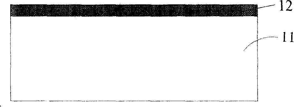
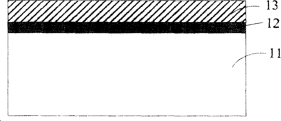
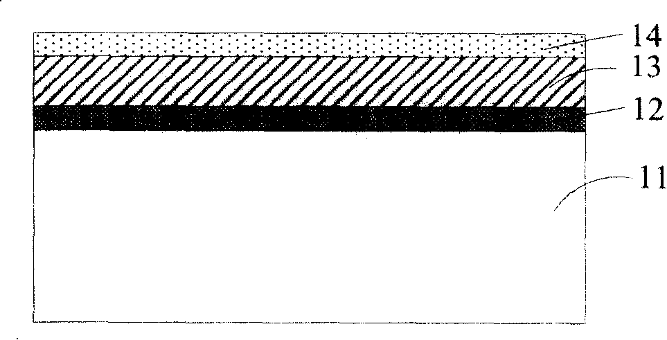
[0038] The present invention firstly provides a method for forming a gate structure, including: sequentially forming a tunnel insulating layer and a first polysilicon layer on a semiconductor substrate; forming a gate structure made of silicon nitride on the first polysilicon layer A first interlayer insulating layer; forming a second interlayer insulating layer made of high-k dielectric on the first interlayer insulating layer; forming a second polysilicon layer on the second interlayer insulating layer.

[0039] refer to figure 1 As shown, it is a schematic structural diagram of forming a tunnel insulating layer 12 on a semiconductor substrate 11 . figure 1 The semiconductor substrate 11 shown in is silicon, and silicon-on-insulator (SOI) can also be used as the semiconductor substrate 11 . The tunnel insulating layer 12 shown in the...


PUM


Abstract

The invention relates to a grid formation method. The invention comprises a tunneling insulating layer, a first polysilicon layer, a first interlayer insulating layer, a second interlayer insulating layer and a second polysilicon layer,which are formed on a semiconductor substrate in sequence, wherein, the first interlayer insulating layer adopts oxygen-rich silicon nitride, and the second interlayer insulating layer adopts high-K dielectrics. The invention provides a gate structure correspondingly, and also provides a semi-conductor memory and the manufacturing method thereof. Because the invention adopts high-K dielectric material as the second interlayer insulating layer to replace silicon nitride and silicon oxide of the ONO in the prior art, and the dielectric constant of the high-K dielectric material is higher than that of the silicon oxide, the thickness of the high K-dielectric material can be reduced, and therefore the area of a storage unit is reduced, simultaneously the higher coupling ratio is kept between the first interlayer insulating layer and the floating gate, and the higher coupling ratio ensures the programmable voltage to be decreased. Thereby the operating voltage of the flash memory is reduced, and the shorter programming/erasing time can be realized.

Description

technical field [0001] The invention relates to the field of semiconductor memory, in particular to a non-volatile semiconductor memory and a forming method thereof. Background technique [0002] Semiconductor storage devices that store data can be classified into volatile storage devices or non-volatile storage devices. Volatile memory devices lose stored data after a power interruption, whereas non-volatile memories can still retain stored data after a power interruption. Flash memory is a typical application of non-volatile memory. A memory cell of a flash memory includes a floating gate and a control gate electrode, and the control gate electrode controls charge injection into or extraction from the floating gate. A non-volatile memory cell generally includes a source region, a drain region, a channel in a substrate, and a stacked gate structure on the channel. The stacked gate includes a gate dielectric layer (usually referred to as a tunnel oxide layer) formed on a ...

Claims


Application Information

Patent Timeline
Patent Type & Authority Applications(China)
IPC IPC(8): H01L21/28H01L21/336H01L21/8247H01L29/51H01L29/78H01L27/115
Inventor 张璋炎
Owner SEMICON MFG INT (SHANGHAI) CORP
Why Eureka
Try Eureka