Process for preparing nano structure of zinc oxide
A zinc oxide nano- and nano-structure technology, applied in nano-structure manufacturing, zinc oxide/zinc hydroxide, nanotechnology, etc., can solve problems such as unrealized position and number controllable
- Summary
- Abstract
- Description
- Claims
- Application Information
AI Technical Summary
Problems solved by technology
Method used
Image
Examples
Embodiment Construction
[0019] The present invention will be described in further detail below in conjunction with the accompanying drawings and a specific embodiment.
[0020] 1. Use n-type high-conductivity single crystal silicon with crystal orientation (resistivity 2.4~3.7×10 -3 Ω·cm)11 as the substrate.
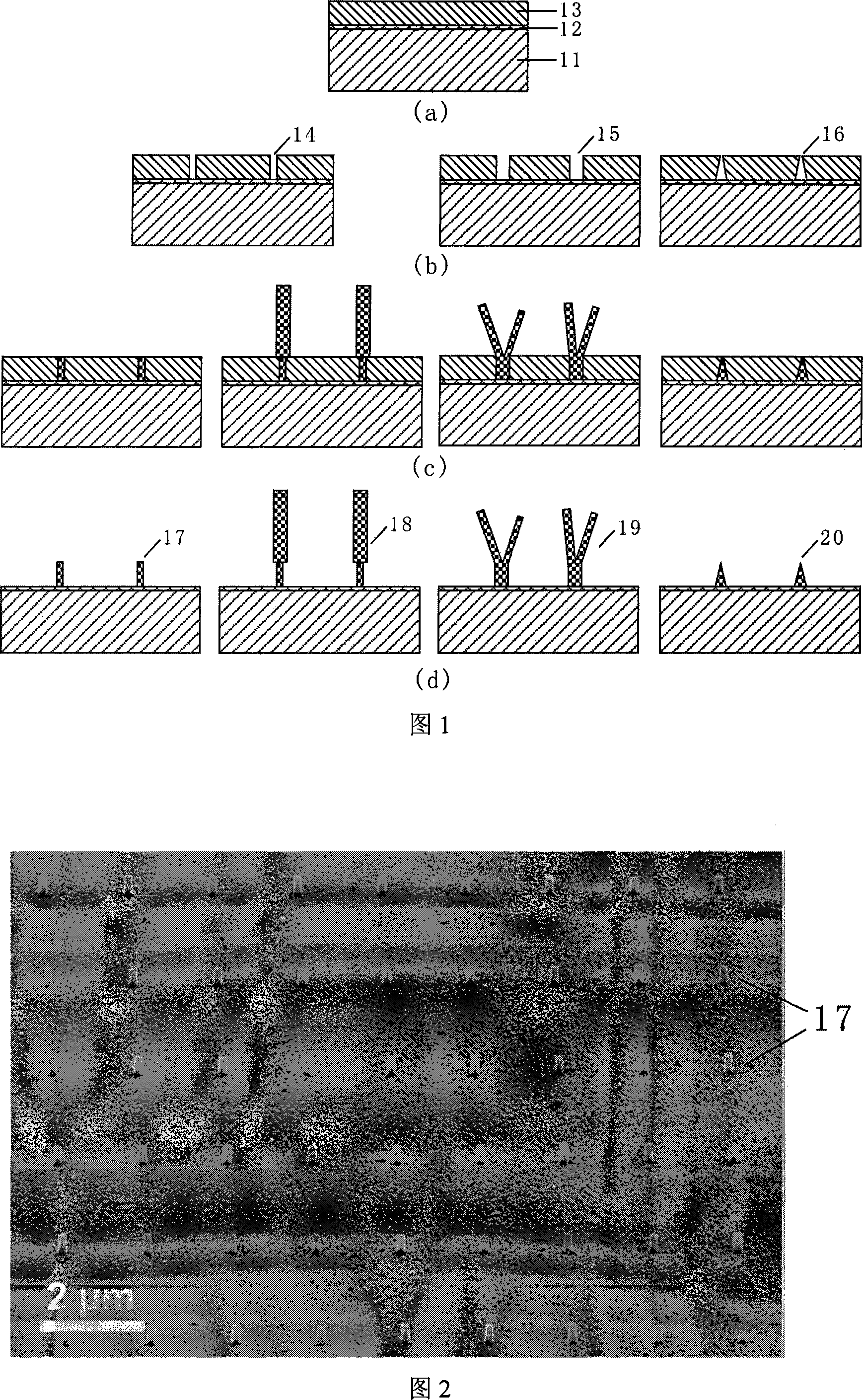
[0021] 2. As shown in Figure 1(a), a 50nm-thick metal zinc (Zn)12 thin film was deposited on a single crystal silicon wafer using a SP-3 magnetron sputtering station. The film preparation conditions are as follows: background vacuum: 3.0×10 -3 Pa; process gas: high-purity argon (Ar) gas (flow rate: 60 sccm); sputtering power: DC sputtering 300W; time: 2 minutes; working temperature: room temperature.
[0022] 3. Use a KW-4AH type hot plate to bake the silicon substrate coated with the metal zinc film at a temperature of 180°C before gluing for 30 minutes.
[0023] 4. Utilize the Karl Suss RC8 glue coating machine, evenly spin-coat the PMMA (950K C4) 13 (Fig. The glue rotation speed is 3000...
PUM
 Abstract
Description
Claims
Application Information


