A deep ditch groove high-power MOS device and the corresponding manufacturing method

A MOS device, high-power technology, applied in the field of deep trench high-power MOS devices and its manufacturing, can solve the problems of device capacitance increase, limitation, device switching speed reduction, etc., to achieve the effect of increasing breakdown voltage and diluting power lines

Inactive Publication Date: 2008-07-09
SUZHOU SILIKRON SEMICON CO LTD
View PDF0 Cites 26 Cited by
  • Summary
  • Abstract
  • Description
  • Claims
  • Application Information

AI Technical Summary

Problems solved by technology

At present, the mass production capacity of unit cell pitch (Pitch) at home and abroad can reach 1.2um~1.7um, the corresponding groove size is 0.4um, and the alignment accuracy requirement of stepper lithography machine is +/-0.12um, 0.9um The ~1.1um unit cell

Method used


Image

  • A deep ditch groove high-power MOS device and the corresponding manufacturing method
  • A deep ditch groove high-power MOS device and the corresponding manufacturing method
  • A deep ditch groove high-power MOS device and the corresponding manufacturing method

Examples


Embodiment

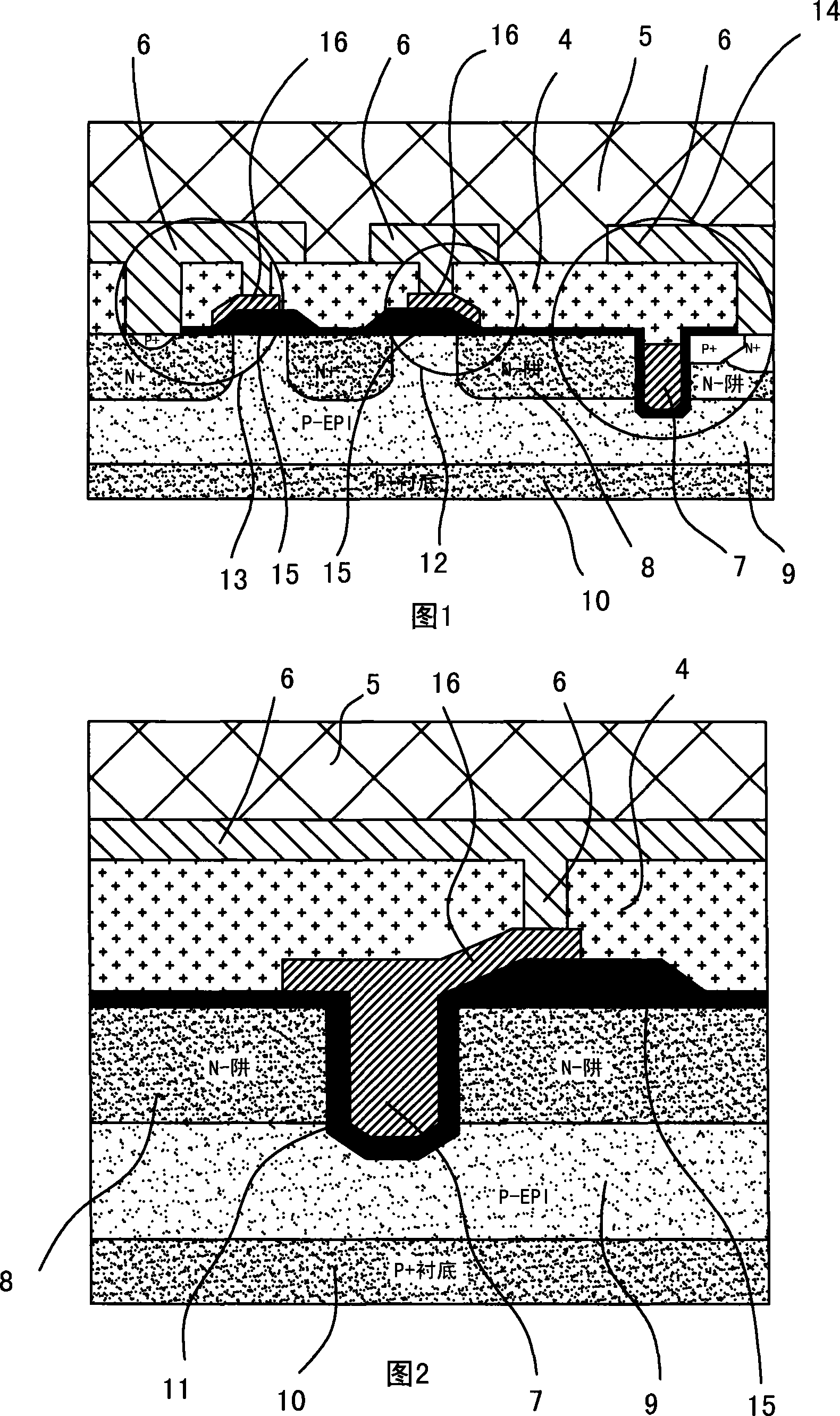
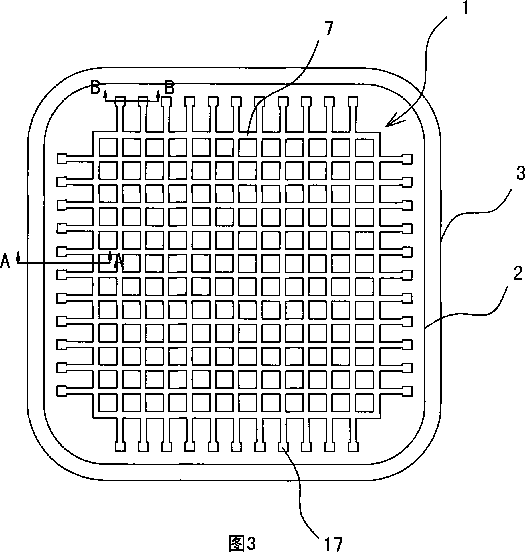
[0054] Embodiment: A deep trench high power P-type MOS device

[0055] 3 is a schematic plan view of a deep trench high-power P-type MOS device in a top view state. It can be seen from the figure that a unit cell array 1 is provided in the central area of ​​the MOS device, and a terminal protection structure is provided on the periphery of the unit cell array 1 . The unit cell array 1 is made of trench-type conductive polysilicon 7 to connect each unit cell in parallel to form a whole. The terminal protection structure is composed of a protection ring 2 located in the inner ring and a cut-off ring 3 located in the outer ring. In this embodiment, there is only one guard ring, but two or more guard ring structures may also be used, which is determined by actual needs.

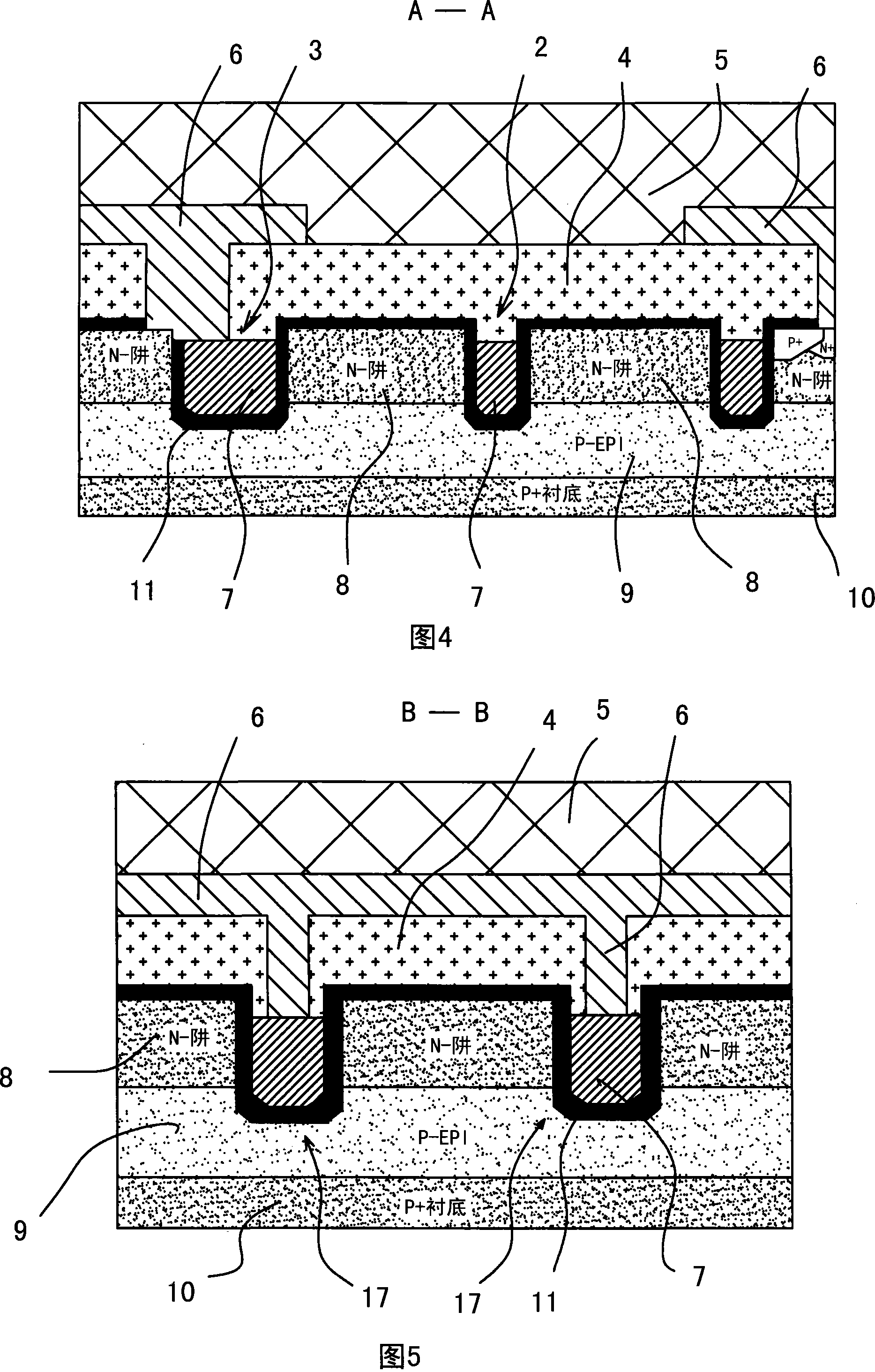
[0056] FIG. 4 is a cross-sectional view of A-A of FIG. 3 , which is a schematic cross-sectional view of a deep trench high-power MOS device according to an embodiment of the present invention. It can be seen f...


PUM


Abstract

The invention relates to a deep trench high-power MOS device and the manufacturing method. The MOS device is arranged on an overlooking plane, a central area is provided with an array which consists of parallel connected single cells, the periphery of the single-cell array is provided with a terminal protection structure, the terminal protection structure consists of at least one protection ring which is arranged at an inner ring and a stop ring which is positioned at an outer ring; as both the protection ring and the stop ring adopt trench type conductive polysilicon, and a single-cell grid electrode lead wire adopts the method of directly opening a hole to lead the wire on the trench type conductive polysilicon in the manufacturing process of the device; compared with the manufacturing method of existing common plane type deep trench high-power MOS device with a field-plate structure, the invention can reduce two lithographys and corresponding processes under the premise of not affecting the performances of the device, thus greatly reducing manufacturing cost. At the same time, the invention adopts one time phosphorus injection, then one time boron injection and matching annealing processes are adopted to regulate the conductive polysilicon resistance, thereby greatly reducing the leakage current between a grid and a source and ensuring to obtain a reasonable threshold voltage under the premise of not increasing the concentration of an N-well.

Description

technical field [0001] The invention relates to a high-power MOS device and a manufacturing method thereof, in particular to a deep-groove high-power MOS device and a manufacturing method thereof. This MOS device adopts the structural design of the trench conductive polysilicon guard ring and the trench conductive polysilicon stop ring, which can be reduced without affecting the device performance (such as specific Rdson, withstand voltage, device capacitance, etc.) The number of photolithography plates, thereby reducing the manufacturing cost of the device. Background technique [0002] The basic requirement of modern deep-trench high-power devices is to be able to withstand high voltage and operate at high current. Among them, the deep trench MOSFET usually achieves high current operation by connecting a large number of trench MOS unit cells in parallel. However, for high-voltage deep trench MOSFETs, the surface potentials of the parallel unit cells located in the middle...

Claims


Application Information

Patent Timeline
IPC IPC(8): H01L27/088H01L23/522H01L21/8234
CPCH01L2924/0002
Inventor 朱袁正秦旭光
Owner SUZHOU SILIKRON SEMICON CO LTD
Why Eureka
Try Eureka