Method for manufacturing dent source leakage field effect transistor
A transistor and leakage field technology, which is applied in the field of manufacturing recessed source-drain field-effect transistors, can solve problems such as inability to introduce stress and difficulties in actual process realization.
- Summary
- Abstract
- Description
- Claims
- Application Information
AI Technical Summary
Problems solved by technology
Method used
Image

Examples
Embodiment Construction
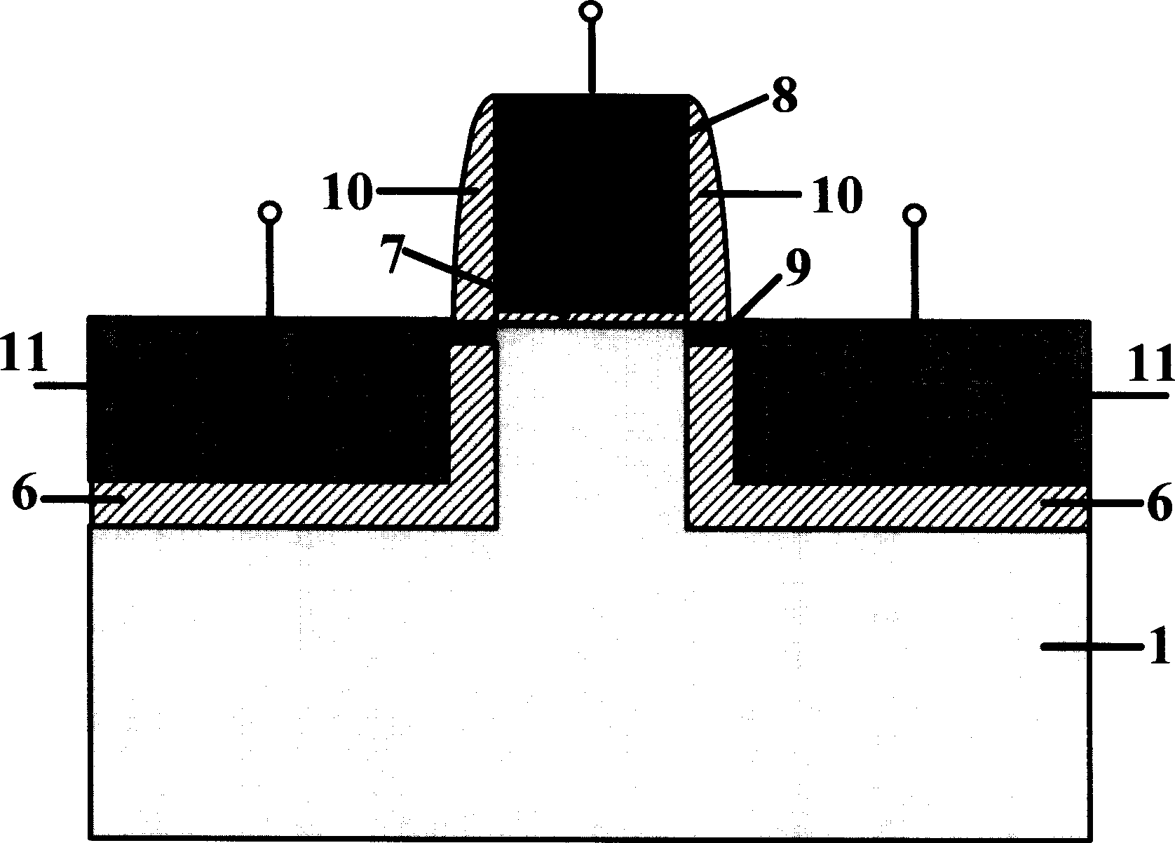
[0028] In the following, we will introduce in detail the implementation process of preparing a recessed source-drain field-effect transistor using the present invention.
[0029] (1) cleaning bulk silicon wafer;
[0030] (2) Deposit a hard mask, and implant doping on the surface of the silicon wafer to form a reversely doped heavily doped region; then remove the hard mask;
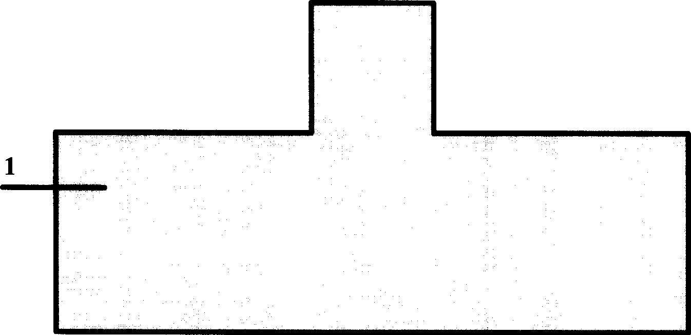
[0031] (3) Deposit photoresist, use the layout of the gate lines as a mask, define the silicon platform by photolithography, and dry etch to obtain a height of H 1 the silicon stage, remove the glue, and get as Figure 2-a structure, H 1 The numerical range of can be between 10 nanometers and 200 nanometers;
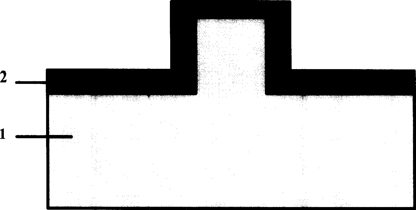
[0032] (4) Clean and remove the natural oxide layer, epitaxially grow germanium silicon (GeSi) material on the silicon surface, and the epitaxial thickness is H 2 , H 2 1 ;Such as Figure 2-b , H 2 The numerical range of can be between 10 nanometers and 100 nanometers;
[0033] (5) Clean and ...
PUM
 Abstract
Description
Claims
Application Information
 - R&D
- Intellectual Property
- Life Sciences
- Materials
- Tech Scout
- Unparalleled Data Quality
- Higher Quality Content
- 60% Fewer Hallucinations
Browse by: Latest US Patents, China's latest patents, Technical Efficacy Thesaurus, Application Domain, Technology Topic, Popular Technical Reports.
© 2025 PatSnap. All rights reserved.Legal|Privacy policy|Modern Slavery Act Transparency Statement|Sitemap|About US| Contact US: help@patsnap.com