Nanometer oxide porous membrane electrode and preparing method and application thereof

A nano-oxide and porous film technology, which is applied in capacitor electrodes, circuits, photovoltaic power generation, etc., can solve the problems of time-consuming, unusable, and energy consumption, and achieve the effects of simple preparation process, energy saving, and uniform film layer

Inactive Publication Date: 2008-07-30
INST OF PHYSICS - CHINESE ACAD OF SCI
View PDF0 Cites 11 Cited by
  • Summary
  • Abstract
  • Description
  • Claims
  • Application Information

AI Technical Summary

Problems solved by technology

This method has the following problems: (1) high temperature treatment, time-consuming and energy-consuming; (2) for flexible dye-sensitized solar cells, this method cannot be used because the polymer flexible substrate used cannot withstand high temperatures above 150 °C

Method used


Image

  • Nanometer oxide porous membrane electrode and preparing method and application thereof
  • Nanometer oxide porous membrane electrode and preparing method and application thereof

Examples


Embodiment 1

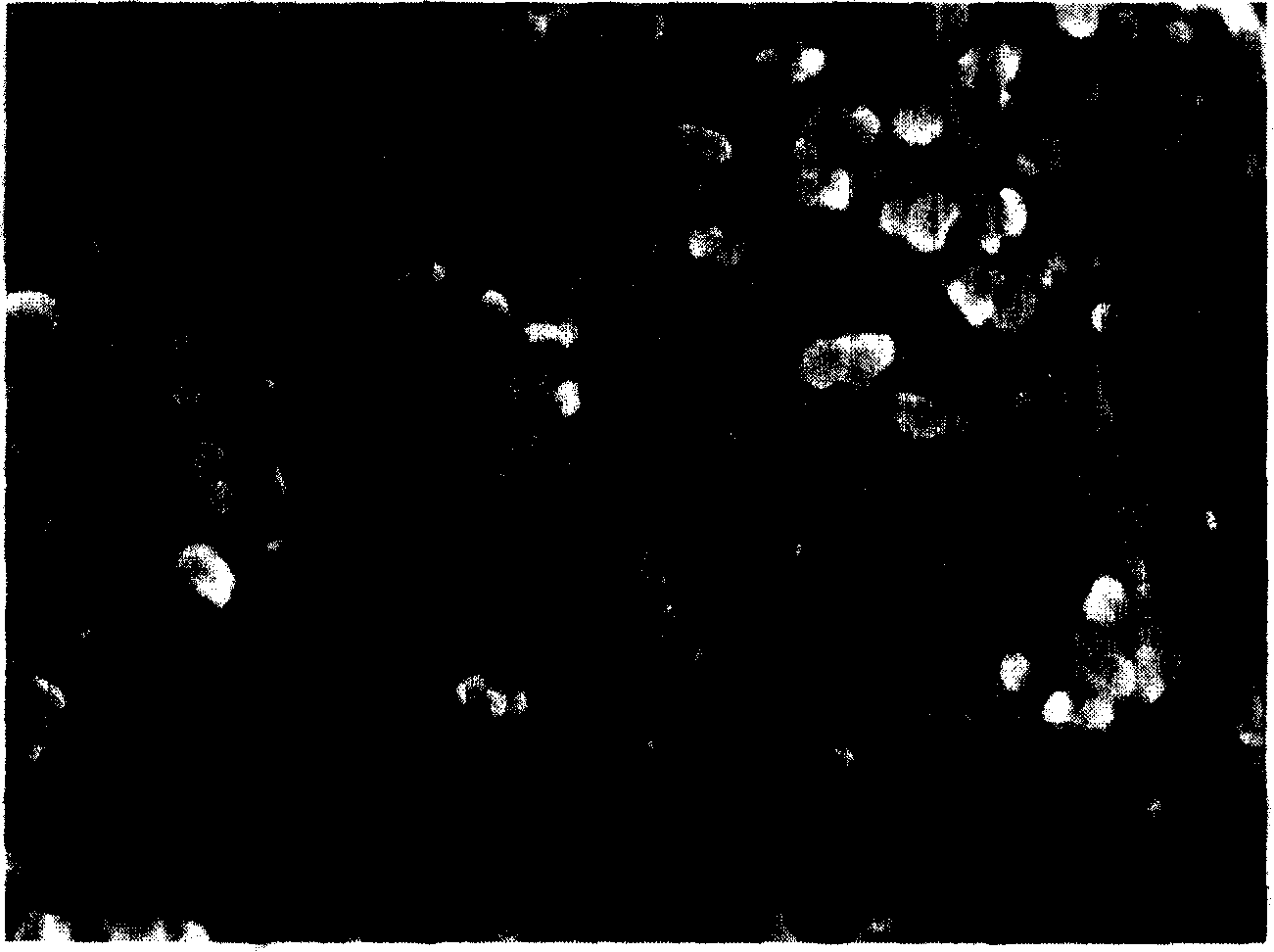
[0036] Present embodiment is made on the FTO glass substrate and is coated with 2 layers of nano-semiconductor material ZnO layers, obtains nano-semiconductor material ZnO porous film, and the aperture of irregular hole is 0.01-2 nanometer; Film thickness is at 1 micron, and film porosity is at 30% , the specific surface area can be 40 square meters per gram.

[0037] The concrete method that present embodiment makes nano-semiconductor material ZnO porous film is as follows:

[0038] 1) preparation solution concentration is the aqueous acetic acid solution of 0.2wt%;

[0039] 2) Mix 3g of ZnO nanopowder (with a particle size of 20 nanometers) with 15g of acetic acid aqueous solution, grind and mix it on a ball mill for 1 hour, then leave it at room temperature for 30 minutes to obtain a nanometer ZnO slurry;

[0040] 3) on the FTO glass substrate, apply the nano-ZnO slurry film prepared in step 2) by scraping, and apply it for 3 times to obtain a film layer with the same semi...

Embodiment 2

[0044] Present embodiment is made on the FTO glass substrate and is coated with 3 layers of nano-semiconductor material ZnO layers, obtains nano-semiconductor material ZnO porous film, and the aperture of irregular hole is 1 nanometer; Film thickness is at 4 microns, and film porosity is at 40%, ratio The surface area can be in the range of 60 m2 / g.

[0045] The concrete method that present embodiment makes nano-semiconductor material ZnO porous film is as follows:

[0046] 1) preparation solution concentration is the acetic acid aqueous solution of 1wt%;

[0047] 2) Mix 3g of ZnO nanopowder (with a particle size of 20 nanometers) with 8g of acetic acid aqueous solution, grind and mix it on a ball mill for 1 hour, then leave it at room temperature for 30 minutes to obtain a nanometer ZnO slurry;

[0048] 3) on the FTO glass substrate, apply the nano-ZnO slurry film prepared in step 2) by scraping, and apply it for 3 times to obtain a film layer with the same semiconductor. Af...

Embodiment 3

[0051] Present embodiment is made on the FTO glass substrate and is coated with 3 layers of nano-semiconductor material ZnO layers, obtains nano-semiconductor material ZnO porous film, and the aperture of irregular hole is 0.1-5 nanometer; Film thickness is at 12 microns, and film porosity is at 40% , the specific surface area can be 60 square meters per gram.

[0052] The concrete method that present embodiment makes nano-semiconductor material ZnO porous film is as follows:

[0053] 1) preparation solution concentration is the acetic acid aqueous solution of 3wt%;

[0054] 2) Mix 3g of ZnO nanopowder (with a particle size of 20 nanometers) with 3g of acetic acid aqueous solution, grind and mix on a ball mill for 1 hour, then leave at room temperature for 30 minutes to obtain a nanometer ZnO slurry;

[0055] 3) On the FTO glass substrate, apply the nano-ZnO slurry film prepared in step 2) by scraping, and apply it for 3 times to obtain a film layer with the same semiconducto...


PUM

PropertyMeasurementUnit
particle diameteraaaaaaaaaa
thicknessaaaaaaaaaa
specific surface areaaaaaaaaaaa

Abstract

The invention relates to a nano-oxide porous thin film electrode and preparation method thereof. The thin film electrode comprises two or more layers of oxide semiconductor thin films applied on a substrate, wherein irregular holes are formed in the thin films with a diameter ranging from 0.01 to 10 nm; the particle diameter of the oxide semiconductor material layer is from 5 to 500 nm; the thickness of the thin film is between 1 mum and 50 mum; and the void rate thereof is between 30% and 60% and a specific surface area thereof is between 40 m<2> / g and 130 m<2> / g. The preparation method of the thin film comprises following steps: (1) preparing an acid solution with a concentration of 0.1 to 5 wt%; (2) preparing a nano-colloid slurry of a semiconductor oxide; (3) applying the nano-colloid slurry of the semiconductor oxide onto the substrate; and (4) activating the thin film in an activator solution.The thin film electrode of the invention is prepared at a room temperature thus greatly saving energy resources which can be used as the photo-anode of flexible solar cell.

Description

technical field [0001] The present invention relates to an oxide film electrode and its preparation method, in particular to a dye-sensitized solar cell and other energy conversion devices, energy storage devices and sensor devices on flexible and non-flexible substrates with high Oxide porous film electrode with active surface and high connectivity, and its low-temperature preparation method. Background technique [0002] At present, due to the constraints of fossil resources and their massive consumption, profound environmental and energy problems are caused, such as global warming, environmental degradation, etc., which directly affect the survival and quality of life of human beings. Human beings urgently need to develop green and safe new energy sources . [0003] One of the solutions to the energy problem is to use solar energy. In one year, the amount of solar energy reaching the earth's surface is enormous, which is equivalent to 10,000 times the annual energy cons...

Claims


Application Information

Patent Timeline
Patent Type & Authority Applications(China)
IPC IPC(8): H01L31/0224H01L31/18H01M14/00H01G9/20H01G9/04
CPCY02E10/542Y02P70/50
Inventor 孟庆波刘喜哲罗艳红李泓陈立泉
Owner INST OF PHYSICS - CHINESE ACAD OF SCI
Why Eureka
Try Eureka