Metal-ceramic composite substrate and method for manufacturing same

A ceramic composite and metal substrate technology, applied in the direction of semiconductor lasers, printed circuits, lasers, etc., can solve the problems of poor heat dissipation, high cost, and poor yield, and achieve small temperature rise, improved heat dissipation, and reduced thermal resistance Effect

Inactive Publication Date: 2008-07-30
DOWA ELECTRONICS MATERIALS CO LTD
View PDF0 Cites 11 Cited by
  • Summary
  • Abstract
  • Description
  • Claims
  • Application Information

AI Technical Summary

Problems solved by technology

However, there is a problem that the sintering process of the ceramic substrate itself is required, the process is complicated, the yield is poor, and the cost is higher than that of the printed circuit board and the metal base substrate of Patent Document 1.
[0007] In addition, if the circuit structure is miniaturized, the thermal resistance per unit volume of the ceramic substrate with low thermal conductivity will be higher than that of the metal substrate with Cu and Al as the substrate.
Therefore, on a small circuit such as a semiconductor element mounted thereon, such as a heat sink (submount), the thermal resistance of the AlN substrate of the entire heat sink is 90% or more, and the heat dissipation performance is deteriorated, so it cannot be said that it is not suitable for heat dissipation.

Method used


Image

  • Metal-ceramic composite substrate and method for manufacturing same
  • Metal-ceramic composite substrate and method for manufacturing same
  • Metal-ceramic composite substrate and method for manufacturing same

Examples


Embodiment

[0093] Hereinafter, the present invention will be described in more detail based on examples.

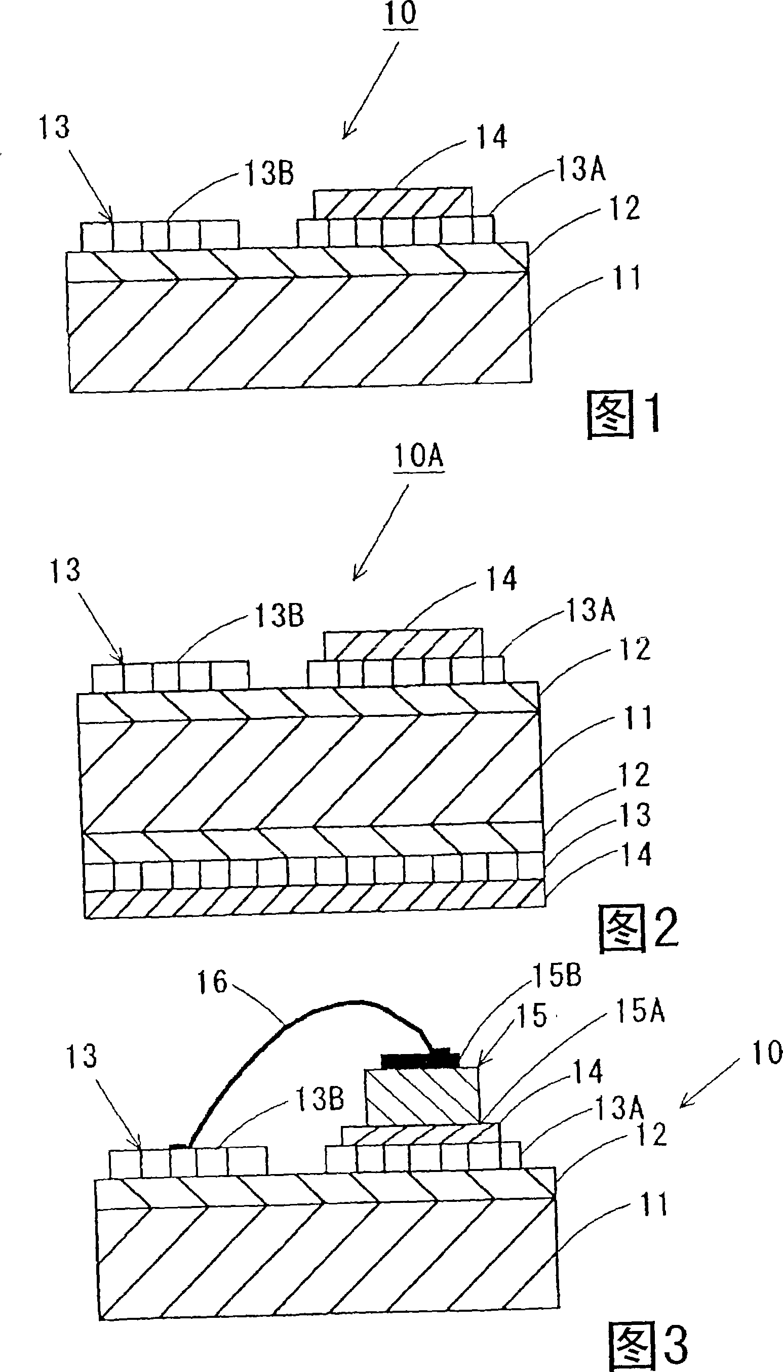
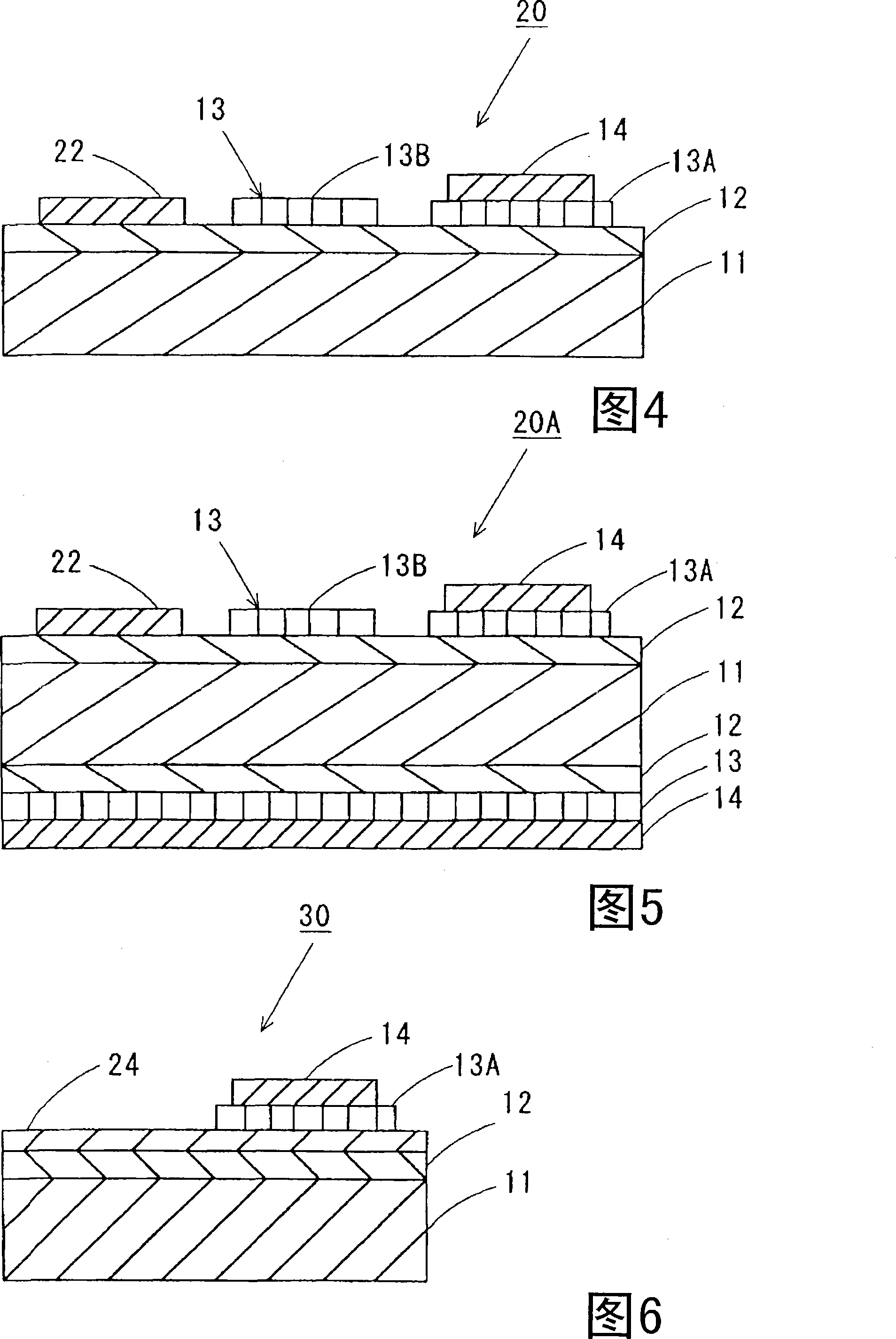
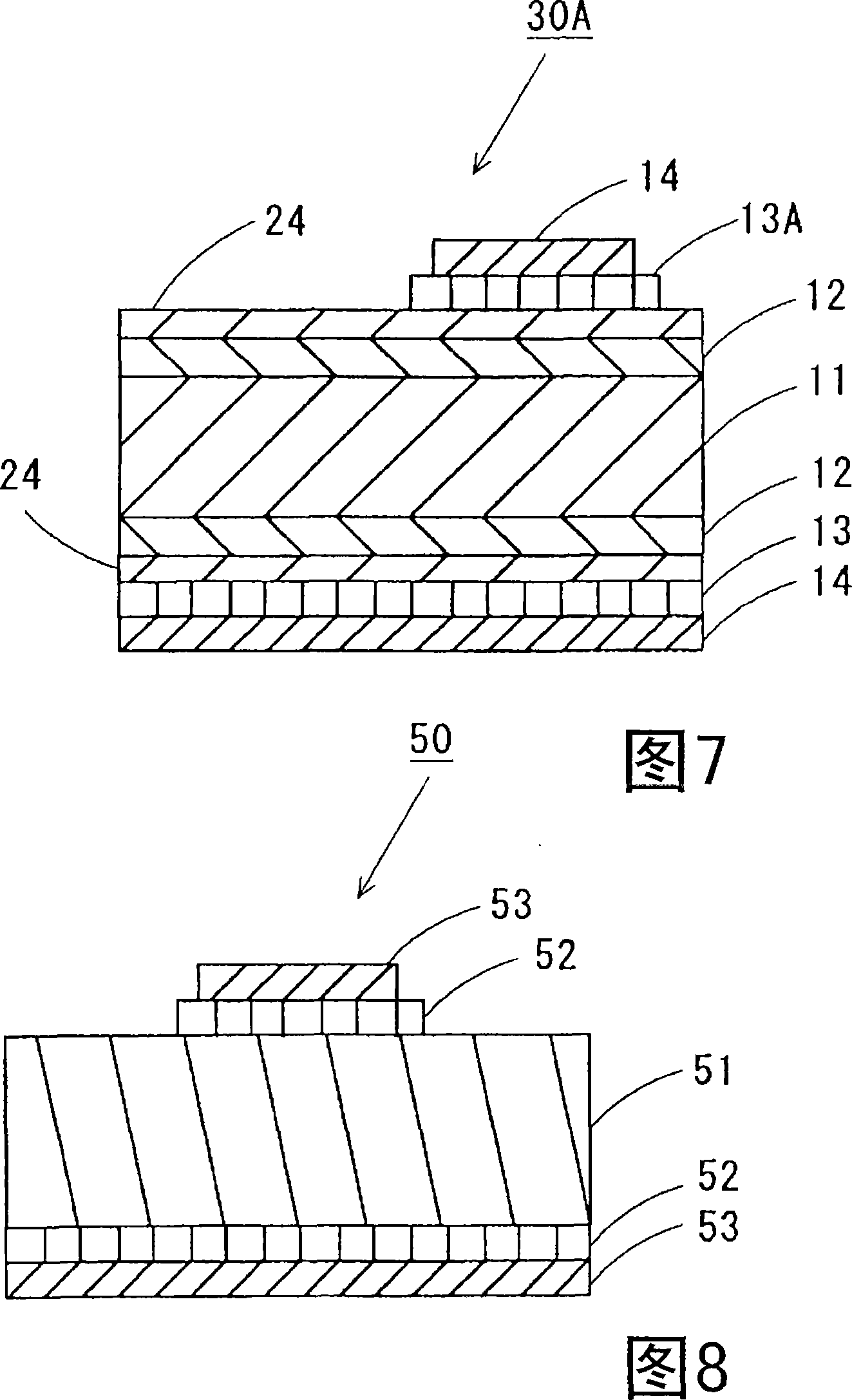
[0094] First, a method of manufacturing the metal-ceramic composite substrate 30A of the example will be described.

[0095] Both surfaces of the metal substrate 11 made of Cu with a size of 50 mm x 50 mm, a thickness of 300 μm, and a thermal conductivity of 300 W / mK were cleaned to perform surface cleaning. A ceramic layer 12 made of AlN with a thickness of 10 μm. As the PVD method, a sputtering apparatus is used. Al is used as a target, and further, an AlN thin film 12 is deposited by simultaneously supplying nitrogen gas. The thermal conductivity of this AlN thin film was 200 W / mK.

[0096] Next, on the entire front and rear surfaces of the AlN thin film 12, Ti was deposited as a ceramic layer protective film 24 with a thickness of 0.05 μm and a thermal conductivity of 20 W / mK by a vacuum deposition apparatus.

[0097] For patterning by photolithography, resist is uniformly c...


PUM

PropertyMeasurementUnit
thicknessaaaaaaaaaa
thicknessaaaaaaaaaa
sizeaaaaaaaaaa

Abstract

A metal-ceramic composite substrate having an excellent heat dissipating characteristic and a method for manufacturing such composite substrate at low cost. The metal-ceramic composite substrate (10) is composed of a metal substrate (11), a ceramic layer (12) formed on the metal substrate (11), an electrode layer (13) formed on the ceramic layer (12), and a solder layer (14) formed on the electrode layer (13). The ceramic layer (12) is composed of a ceramic thin film. When the ceramic layer (12) is formed of an aluminum nitride thin film, the metal-ceramic composite substrate (10) having the excellent heat dissipating characteristic is provided for an electronic circuit.

Description

technical field [0001] The present invention relates to a metal-ceramic composite substrate used as a substrate for electronic circuits and a method for producing the same. Background technique [0002] Generally, various electronic components are mounted and soldered at predetermined positions on a copper wiring pattern formed on a printed circuit board, and electronic circuits are connected. However, since various resins such as paper phenolic resin, epoxy resin, and glass epoxy resin are used as the material of the printed circuit board, although it is low in cost, heat dissipation is not good. [0003] Patent Document 1 discloses a circuit board for mounting a semiconductor in which an insulating filler is poured into a patterned metal base substrate of Al, Cu, or the like to form a circuit in order to achieve high-density mounting of the circuit board for mounting a semiconductor. In this document, a silicon-containing epoxy resin having a thickness of 100 μm is used a...

Claims


Application Information

Patent Timeline
Patent Type & Authority Applications(China)
IPC IPC(8): H01L23/12H01L23/36H01S5/022
CPCH01L23/142H01L23/15H01L23/3735H01L24/28H01L24/45H01L24/48H01L24/83H01L2224/29144H01L2224/45144H01L2224/48472H01L2224/83192H01L2224/83801H01L2924/01079H01L2924/14H01S5/02476H05K1/053H05K2201/0179H01L2924/12041H01L2224/32225H01L2224/48091H01L2224/48227H01L2224/73265H01L2924/1301H01L2924/12042H01L2924/00011H01L2224/85424H01L2224/85439H01L2224/85444H01L2224/85447H01L2224/8546H01L2224/85466H01L2224/85469H01L2224/85484H01S5/0237H01L2924/00014H01L2924/0105H01L2924/00H01L2924/01047H01L2924/01004
Inventor 大鹿嘉和
Owner DOWA ELECTRONICS MATERIALS CO LTD
Why Eureka
Try Eureka