Nanocrystalline silicon forming method

A nanocrystalline silicon and nanotechnology, which is applied in the field of vacuum deposition of nanocrystalline silicon thin films, can solve problems such as damage to the performance of nanocrystalline silicon thin film devices, and achieve the effects of reducing cross-contamination and short exposure time.

Inactive Publication Date: 2008-08-20
BEIJING XINGZHE MULTIMEDIA TECH
View PDF0 Cites 3 Cited by
  • Summary
  • Abstract
  • Description
  • Claims
  • Application Information

AI Technical Summary

Problems solved by technology

The traditional method of continuously generating hydrogenated silicon to generate nanocrystalline silicon inevitably leads to the formation of an amorphous silicon conversion layer at the initial stage of hydrogenated silicon formation, severely compromising the performance of nanocrystalline silicon thin film devices requiring minimal transition or conversion materials

Method used


Image

  • Nanocrystalline silicon forming method

Examples


Embodiment Construction

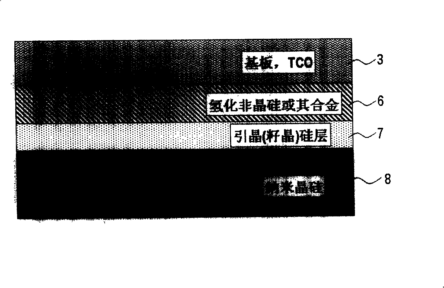
[0021] In the invention, two separate stages composed of different plasma conditions are used to carry out the plasma enhanced chemical vapor deposition process to form a nanocrystalline silicon film.

[0022] As shown in the figure, the first stage is the seeding stage of performing a near-static etching operation on the surface of the formed amorphous silicon film 6 . An intense plasma rich in hydrogen with a small amount of silicon species is maintained for a period of time between 30-600 seconds with a gas mixture high in hydrogen and at the same time silicon-containing gas. For example, a hydrogen and silane (H 2 +SiH 4 ) gas mixture. The gas pressure in the deposition chamber is kept in the range of 0.5-30mbar, preferably in the range of 2-10mbar. The plasma excitation method can be direct current, radio frequency or radio frequency (RF) or very high frequency (VHF). Greater than 150mW / cm 2 A fairly high plasma power density, preferably greater than 250mW / cm 2 , is...


PUM


Abstract

The invention relates to the forming of a nanocrystalline silicon thin film without an amorphous latency layer, which consists of two plasma enhanced chemical vapor deposition stages, namely a dynamic equilibrium hydrogen ion etching preparation stage and a real growing stage thereafter. In a first etching stage, a moulding board which is composed of pint-sized seed crystals (crystal nucleus) forms on the surface based on the silicon thin film; in order not to form amorphous material and miscible thin film at the initial period of the growing stage, nanocrystalline silicon is immediately formed for preparation. The nanocrystalline silicon with an obvious abrupt interface is extremely important for the good transfer efficiency of a thin film silicon solar battery.

Description

technical field [0001] The invention belongs to the field of solar photovoltaic power generation materials, in particular to the vacuum deposition technology of nanocrystalline silicon thin films. Background technique [0002] In recent years, the development of photovoltaic cells and large-area photovoltaic templates (modules) has attracted widespread attention in the world. Hydrogenated amorphous silicon and nanocrystalline silicon, in particular, have shown great potential with the widespread adoption of photovoltaic devices in commercial and residential installations. A notable feature of producing thin-film silicon photovoltaic devices at such a low temperature below 260°C is that the large-area deposited silicon-related semiconductor film layers and electrical contact film layers have excellent performance. At the same time, using well-established coating equipment and procedures, low-cost stencils can be produced industrially. The laser patterning process of differe...

Claims


Application Information

Patent Timeline
Patent Type & Authority Applications(China)
IPC IPC(8): C30B29/06C30B25/00
Inventor 李沅民马昕
Owner BEIJING XINGZHE MULTIMEDIA TECH
Why Eureka
Try Eureka