Production method of miniature radiation detection chip

A technology of radiation detection and manufacturing method, which is applied in the field of electrical replacement of absolute radiometers and the production of micro-radiation detection chips, which can solve the problems of large influence of lead wire resistance, low sensitivity of thermopile ring, large detectable power, etc., and achieve sensitivity and response Increased temperature, good long-term stability, and rapid heat transfer

Active Publication Date: 2008-08-20
JILIN OPTOELECTRONICS ENTERPRISE INCUBATOR
View PDF0 Cites 11 Cited by
  • Summary
  • Abstract
  • Description
  • Claims
  • Application Information

AI Technical Summary

Problems solved by technology

This kind of conical cavity detector has large volume and large heat capacity, so the heat conduction between the conical cavity and the heat sink shell is slow, the time constant of the radiometer is long, and the time to complete a measuremen

Method used


Image

  • Production method of miniature radiation detection chip
  • Production method of miniature radiation detection chip
  • Production method of miniature radiation detection chip

Examples


Embodiment Construction

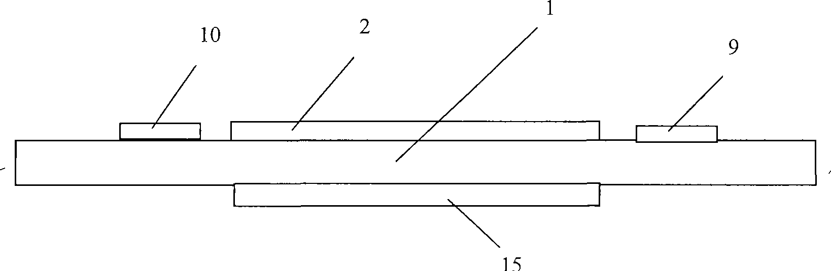
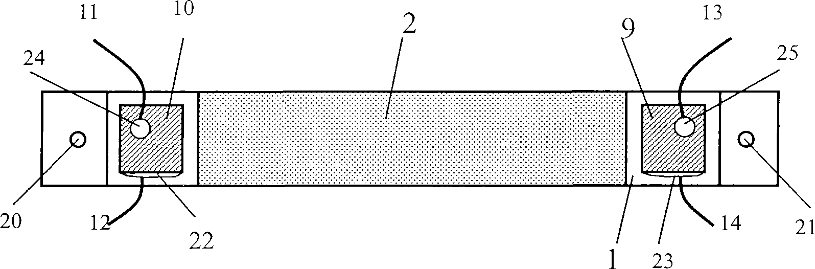
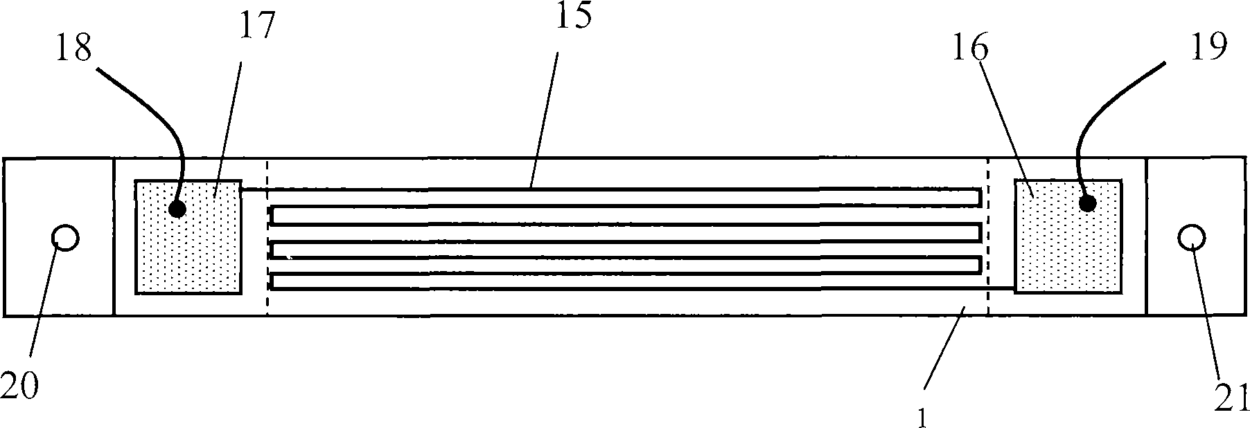
[0026] like figure 2 , 3As shown, the miniature radiation detection chip made by the present invention includes a substrate 1, a radiation absorbing material 2, thermistors 9, 10, thermistor upper electrode leads 11, 13, thermistor lower electrode leads 12, 14, heating wire 15. Heating wire pressure points 16, 17, heating wire leads 18, 19, holes 20, 21, conductive adhesive materials 22, 23 for the thermistor lower electrode, and conductive adhesive materials 24, 25 for the thermistor upper electrode. The substrate 1 is a rectangular sheet with a certain thickness, and its upper and lower surfaces are respectively called a surface and b surface. Surface a of the substrate 1 is distributed with radiation absorbing material 2, thermistors 9, 10, thermistor upper electrode leads 11, 13, thermistor lower electrode leads 12, 14, holes 20, 21, thermistor lower electrodes Conductive adhesive materials 22, 23 and conductive adhesive materials 24, 25 for the upper electrode of the t...


PUM

PropertyMeasurementUnit
Resistivityaaaaaaaaaa
Roughaaaaaaaaaa
Surface roughnessaaaaaaaaaa

Abstract

The present invention relates to a method for preparing a miniature radiation detecting chip, and the method comprises the following steps: preparing a substrate; growing radiation absorbing material on the surface of the substrate; bonding the thermistor on the substrate surface; depositing the heating wire material on the substrate surface; and growing protecting film of the heating wire on the substrate which is provided with a heating wire material film. The structure of the radiation detecting chip prepared by the method of the invention is simple, the dimension and quality are all well controlled; as the substrate adopts the material which has the advantages of high heat conductivity, high insulating property and low heat capacity, and the heating wire and radiation-absorbing material are firmly integrated on the substrate with a MEMS method, the techniques of pasting and the like are not used therefore the heat transmission can be faster. The radiation detecting chip prepared by the method of the invention can be used as the novel embedded scaling reference source on the spacecraft and can also be applied to other thermal radiation detecting fields.

Description

technical field [0001] The invention belongs to the field of optical radiometric measurement, relates to an electrical substitution absolute radiometer, in particular to a method for manufacturing a miniature radiation detection chip used for measuring solar radiation on a satellite. Background technique [0002] The measurement principle of the absolute radiometer is to use the photoelectric equivalence to compare the thermal effect of the unknown irradiance irradiated on the absolute radiometer with the thermal effect of the known electric power (measure the heating current intensity and voltage), so that the heating electric power is equivalent to Received radiated power, calibrated with the method of electrical power reproduction to calibrate the radiation scale. A major application of absolute radiometers is monitoring changes in total solar irradiance onboard spacecraft. [0003] At present, the absolute radiometer mainly adopts double-cone cavity electric replacement...

Claims


Application Information

Patent Timeline
IPC IPC(8): G01J5/02G01J5/20
Inventor 梁静秋方伟梁中翥
Owner JILIN OPTOELECTRONICS ENTERPRISE INCUBATOR
Why Eureka
Try Eureka