

Metal microgrid transparent electrode and method for producing the same
A technology of transparent electrodes and micro-grids, applied in metal material coating process, circuits, electrical components, etc., can solve the problems of complex preparation process of transparent electrodes, low transmittance in the ultraviolet band, high resistivity, and achieve good electrical conductivity. , low cost, high transmittance effect
- Summary
- Abstract
- Description
- Claims
- Application Information
AI Technical Summary
Problems solved by technology
Method used
Image

Examples
Embodiment 1
[0019] Embodiment 1, preparation Ni microgrid transparent electrode
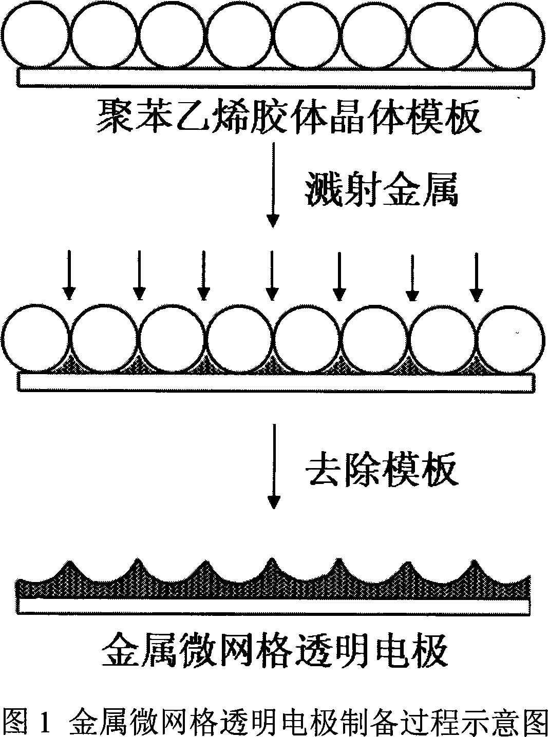
[0020] 1. Using monodisperse polystyrene microspheres with a particle size of 1.4 μm to assemble a monolayer colloidal crystal template
[0021] 2. Using the magnetron sputtering method, metal Ni is deposited on the surface of the template, the working pressure is 0.5Pa, and the power is 40W
[0022] 3. The sputtering stopped after 5 minutes, and Ni was uniformly filled in the gap of the single-layer colloidal crystal template.
[0023] 4. Put the Ni-filled template into the toluene solution for ultrasonic treatment
[0024] 5. Stop after 30 minutes of sonication
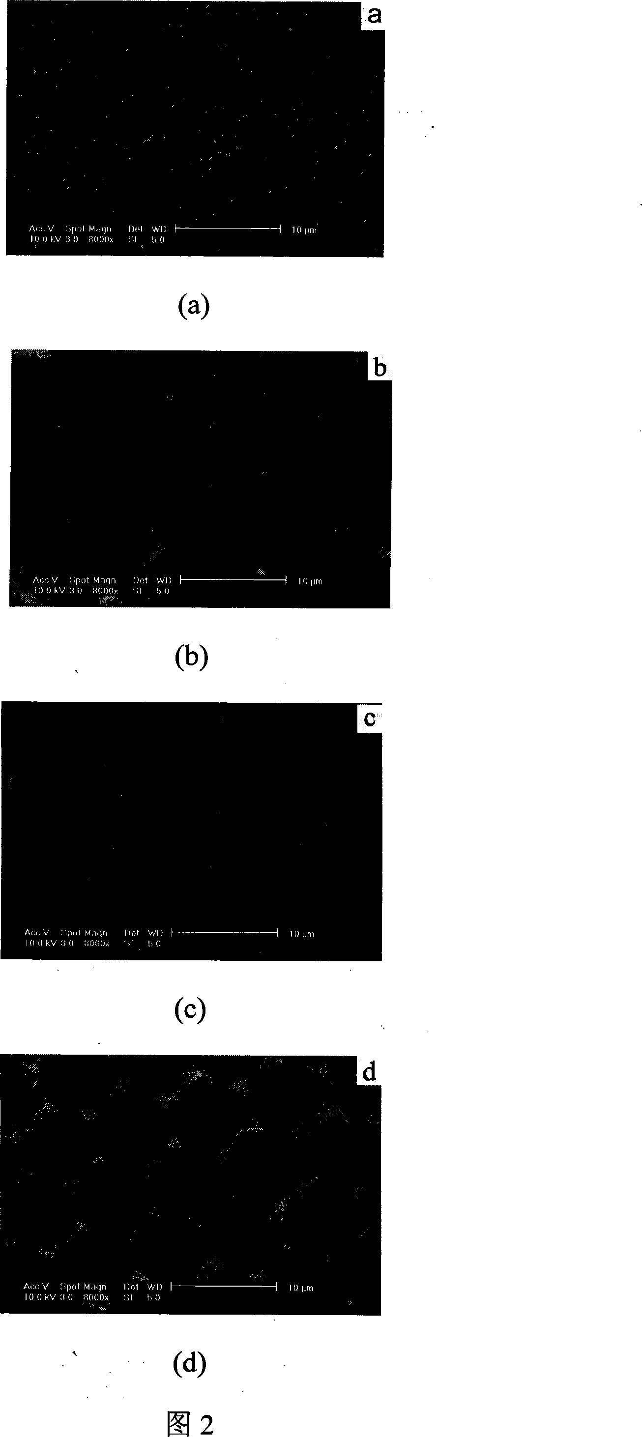
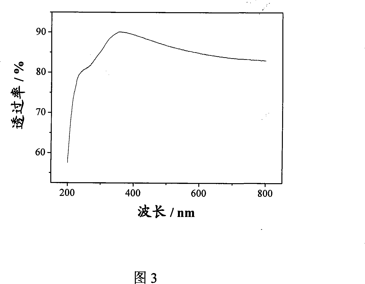
[0025] 6. Take it out from the toluene solution and dry it to obtain a highly ordered Ni microgrid transparent electrode (as shown in Figure 3): pore size, 1.2 μm (as shown in Figure 2 (a)); grid thickness , 10nm; grid width, 140nm.
Embodiment 2
[0026] Embodiment 2, preparation of Al microgrid transparent electrode
[0027] 1. Using monodisperse polystyrene microspheres with a particle size of 3.9 μm to assemble a monolayer colloidal crystal template
[0028] 2. Using the magnetron sputtering method, metal Al is deposited on the surface of the template, the working pressure is 0.5Pa, and the power is 50W
[0029] 3. The sputtering stopped after 5 minutes, and Al was uniformly filled in the gap of the single-layer colloidal crystal template.
[0030] 4. Put the template filled with Al into the toluene solution for ultrasonic treatment
[0031] 5. Stop after 30 minutes of sonication
[0032] 6. Take it out from the toluene solution and dry it to obtain a highly ordered Al microgrid transparent electrode: aperture, 3.4 μm (as shown in Figure 2 (b)); grid thickness, 25nm; grid width, 250nm.
Embodiment 3
[0033] Embodiment 3, preparation silver Ag micro grid transparent electrode
[0034] 1. Using monodisperse polystyrene microspheres with a particle size of 5.1 μm to assemble a monolayer colloidal crystal template
[0035] 2. Use the magnetron sputtering method to deposit metal Ag on the surface of the template, the working pressure is 0.5Pa, and the power is 80W
[0036] 3. The sputtering stopped after 8 minutes, and Ag was uniformly filled in the gap of the single-layer colloidal crystal template.
[0037] 4. Put the Ag-filled template into the toluene solution for sonication
[0038] 5. Stop after 30 minutes of sonication
[0039] 6. Take it out from the toluene solution and dry it to obtain a highly ordered Ag microgrid transparent electrode: aperture, 4.5 μm (as shown in Figure 2 (c)); grid thickness, 30nm; grid width, 580nm.
PUM
| Property | Measurement | Unit |
|---|---|---|
| Particle size | aaaaa | aaaaa |
| Aperture | aaaaa | aaaaa |
| Particle size | aaaaa | aaaaa |
Abstract
Description
Claims
Application Information