Method for insulating AlGaN / GaN HEMT device

A device and substrate technology, applied in the field of microelectronics, can solve problems such as poor electrical isolation, material damage, and large leakage, and achieve good electrical isolation, avoid damage, and achieve good isolation effects

Inactive Publication Date: 2008-08-27
XIDIAN UNIV
View PDF0 Cites 7 Cited by
  • Summary
  • Abstract
  • Description
  • Claims
  • Application Information

AI Technical Summary

Problems solved by technology

[0010] Regardless of whether dry etching isolation or ion implantation isolation is used, there are certain problems at present, which are mainly reflected in two aspects. One is that the electrical isolation effect is

Method used


Image

  • Method for insulating AlGaN / GaN HEMT device
  • Method for insulating AlGaN / GaN HEMT device

Examples


Embodiment Construction

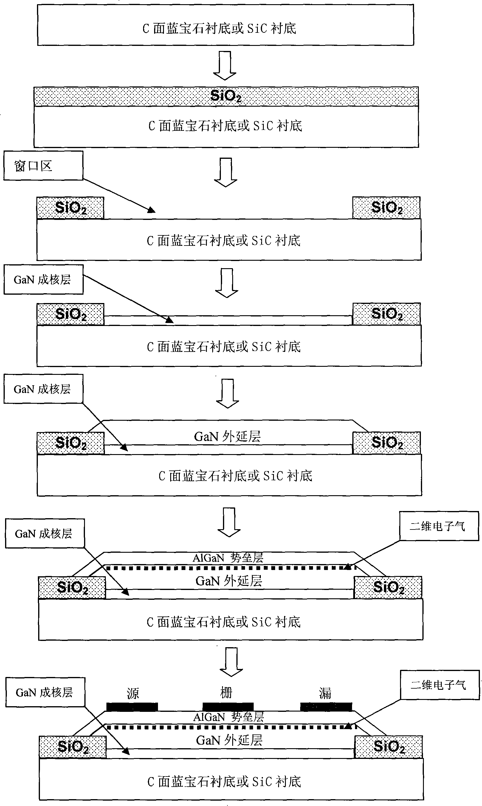
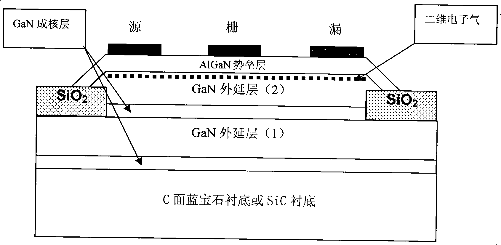
[0025] refer to figure 1 , which is a schematic diagram of the manufacturing process of an AlGaN / GaN HEMT device realized by the isolation method of the present invention. In the manufacturing process, the materials used are: the epitaxial materials are AlGaN and GaN; the substrate material is single crystal sapphire or SiC; the metal material It is Ti / Al / Ni / Au, Ni / Au; the dielectric material is SiO 2 . The process of making a device using the isolation method of the present invention is as follows:

[0026] 1. To Al 2 o 3 The substrate or SiC substrate uses PECVD equipment to deposit SiO with a thickness of about 250nm 2 Layer, PECVD deposition film formation RF frequency is 13.56MHz, power density is 0.011W / cm 2 , the substrate temperature is 350°C, and the reaction chamber pressure is 46.55Pa;

[0027] 2. Spin the glue on the sample at a speed of 5000 rpm, then bake in an oven at 80°C for 10 minutes, and form the window required for etching through photolithography an...


PUM

PropertyMeasurementUnit
Thicknessaaaaaaaaaa
Thicknessaaaaaaaaaa

Abstract

The invention discloses an isolation method for an AlGaN/GaN HEMT device, belonging to the microelectronic technical field. The invention aims to avoid material damage in the isolation technology of the prior device by adoption of the method. The method is realized as follows: selective epitaxial growth GaN base materials are taken as the core; a spacer medium film is deposited on a sapphire or a Sic substrate at first; the spacer medium film is selectively etched according to a design mask, and areas of the medium film which are exposed out of the substrate surface are removed, namely a window area is an active area of the device and the spacer medium film is kept on the outside of the active area; growth of a GaN epitaxial layer and an AlGaN/GaN heterostructure is continued by adoption of the MOCVD technology; the AlGaN/GaN heterostructure only grows in the window area and the surface of a medium film area is only provided with GaN polycrystalline particles and AlGaN polycrystalline particles, thereby isolation of the active area is formed, namely isolation of the device and growth of the materials are completed simultaneously. The invention can be used for manufacturing high performance heterostructure devices, high-power devices and so on.

Description

technical field [0001] The invention belongs to the field of microelectronic technology and relates to semiconductor materials and device manufacturing technology, in particular to an isolation method for AlGaN / GaN HEMT devices, which can be used to manufacture high-performance heterostructure devices and high-power devices. Background technique [0002] In recent years, GaN-based semiconductors have attracted much attention due to their superior physical and chemical properties such as wide bandgap, high critical breakdown field strength, high carrier saturation rate, high thermal conductivity, and high chemical stability. In the GaN-based semiconductor material system, the AlGaN / GaN heterostructure material not only has the above-mentioned superior physical and chemical properties, especially because of the strong polarization effect, a two-dimensional structure with high mobility and high surface density is formed in the heterostructure. The electron gas makes the heteros...

Claims


Application Information

Patent Timeline
IPC IPC(8): H01L21/82H01L21/762H01L21/335
Inventor 张进城董作典郝跃郑鹏天秦雪雪刘林杰王冲冯倩
Owner XIDIAN UNIV
Why Eureka
Try Eureka