Method for manufacturing IGBT silicon epitaxial wafer

A kind of manufacturing method, technology of silicon epitaxial wafer

Active Publication Date: 2008-09-03
NANJING GUOSHENG ELECTRONICS
View PDF0 Cites 43 Cited by
  • Summary
  • Abstract
  • Description
  • Claims
  • Application Information

AI Technical Summary

Problems solved by technology

[0006] Due to the large vapor pressure of the P-type dopant element boron and the large diffusion coefficient in silicon, the self-doping phenomenon of the heavily doped P-type substrate is more obvious during the epitaxial high temperature process, and the special N of the silicon epitaxial wafer for IGBT - / N + / P + Multi-layer structure, the epitaxial process is much more difficult than conventional epitaxial varieties, mainly reflected in: a. Inverse epitaxial, the conductivity type of the epitaxial layer is opposite to that of the substrate, there is a certain compensation, and the transition zone between the epitaxial layer and the substrate is difficult to accurately control ; b, double-layer epitaxy, the resistivity differs by more than 2 orders of magnitude, and it is extremely difficult to control the uniformity and repeatability of the resistivity of the epitaxial layer; c, thick epitaxial layer, it is easy to cause edge warping of the silicon wafer, and the density of lattice defects increases; d. The special epitaxial structure increases the difficulty of testing the resistivity, thickness and longitudinal distribution of the epitaxial layer

Method used


Image

  • Method for manufacturing IGBT silicon epitaxial wafer
  • Method for manufacturing IGBT silicon epitaxial wafer
  • Method for manufacturing IGBT silicon epitaxial wafer

Examples


Embodiment Construction

[0017] The specific embodiment of the present invention is described in detail below:

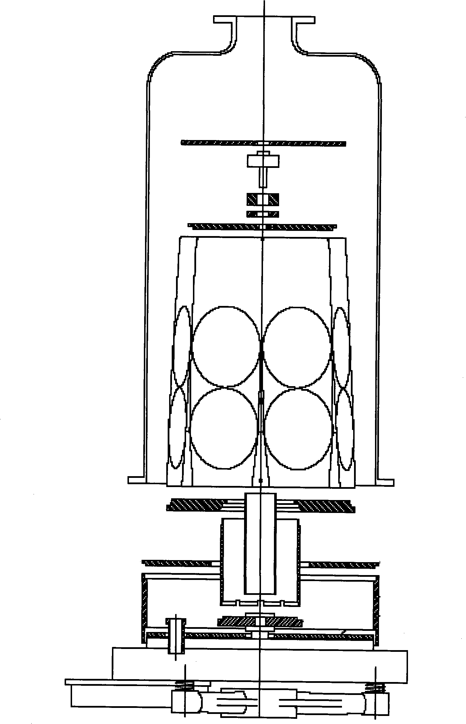
[0018] The equipment used in the present invention is Italy PE-2061S normal pressure silicon epitaxial growth system, see figure 1 , the high-purity graphite base is used as a high-frequency induction heating body, and the main carrier gas is H 2 The purity is above 99.9999%.

[0019] Reactor cleaning: The quartz bell jar and the quartz parts used in the reaction chamber must be carefully cleaned before epitaxy, and the deposition residue on the inner wall of the quartz bell jar and the quartz parts must be thoroughly removed.

[0020] High-temperature treatment in the reaction chamber: Before epitaxial growth, the graphite base must be subjected to HCl high-temperature treatment to remove residual reactants on the base and deposit a layer of intrinsic polysilicon.

[0021] Vapor phase polishing: before epitaxial growth, perform HCl polishing and corrosion on the substrate to remove mecha...


PUM

PropertyMeasurementUnit
purityaaaaaaaaaa

Abstract

The present invention discloses a manufacturing method of IGBT silicon epitaxial wafer, the selecting P type of the heavily Boron-doped & 1t; 100 &g t; the polished piece, the electrical resistivity <= 0.02 Omega cm, the partial flatness <= 1.5 mm, the backing layer of oxide at side edge without the width <= 1mm; appropriate increasing polished time and improving the technique temperature, selecting appropriate HC1 flow quantity 8-10L at 1180 EDG C, polishing time 10 min, sweeping more than 10min by using high flow rate H2 after polishing; synthetic considering factors such as self-doping, crystal lattice quality, electric resistivity control and production efficiency, etc, selecting appropriate epitaxial process condition with double-layer, silicon source using ultra-pure trichlorosilane, first step developing temperature 1080-1100 EDG C, developing rate-controlling 0.8-1.0 Mu m, second step developing temperature 1120-1150 EDG C, developing rate-controlling 1.2-1.6 Mu m, the double-layer epitaxial growth controlled by different adulterate source accurately.

Description

1. Technical field [0001] The present invention relates to semiconductor basic material------silicon epitaxial wafer, specifically, it relates to a manufacturing method of a new type of power electronic device IGBT (insulated gate bipolar transistor) silicon epitaxial wafer. 2. Background technology [0002] IGBT (Insulated Gate Bipolar Transistor) is the core component of high-frequency and high-current electronic power devices. It has the advantages of high input impedance, on-state voltage drop, simple drive circuit, wide safe working area, and strong current handling capability. It overcomes the disadvantage of large on-resistance of VDMOS, and is compatible with the advantages of MOS and bipolar devices. It is very popular among circuit designers. There are more and more applications in many fields of loss, and it has become a promising competitor in the field of power electronic devices. [0003] In order to reduce costs and improve device performance, IGBT has made r...

Claims


Application Information

Patent Timeline
Patent Type & Authority Applications(China)
IPC IPC(8): H01L21/331
Inventor 谭卫东马利行金龙
Owner NANJING GUOSHENG ELECTRONICS
Why Eureka
Try Eureka