Touch screen electrode preparation method
An electrode manufacturing and electrode technology, which is applied in the field of touch film screen electrode manufacturing, can solve problems such as affecting electrical properties, large changes in the contact resistance between electrodes and resistive layers, and exceeding the linearity of a four-wire resistive touch screen.
- Summary
- Abstract
- Description
- Claims
- Application Information
AI Technical Summary
Problems solved by technology
Method used
Image
Examples
Embodiment 1
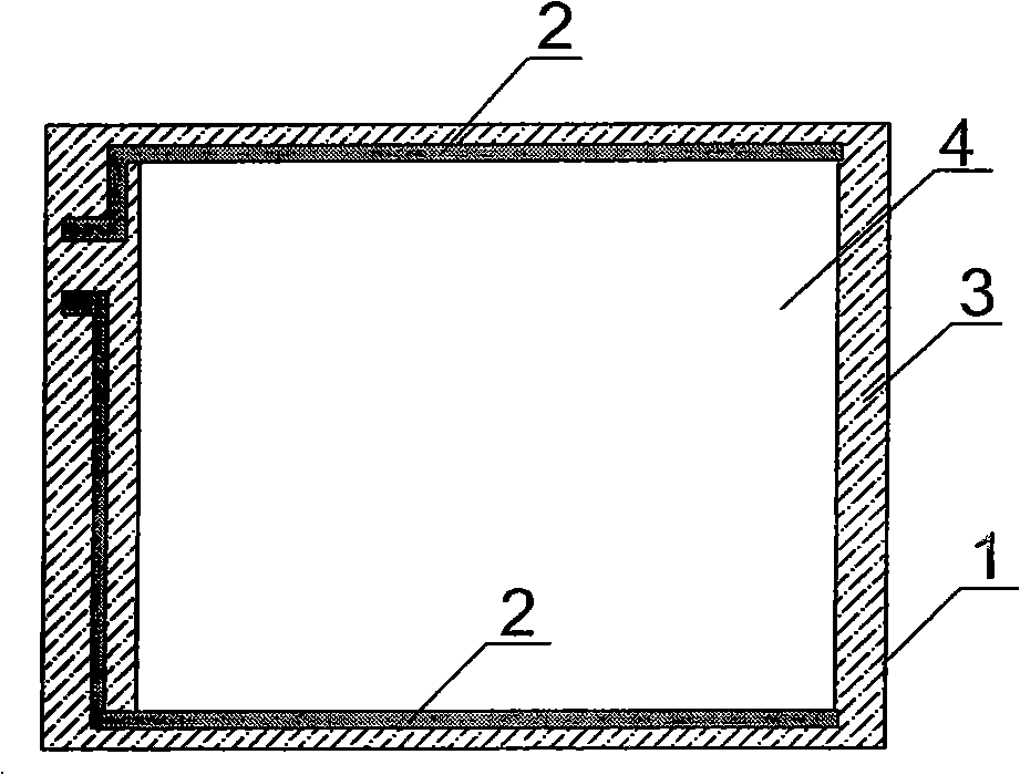
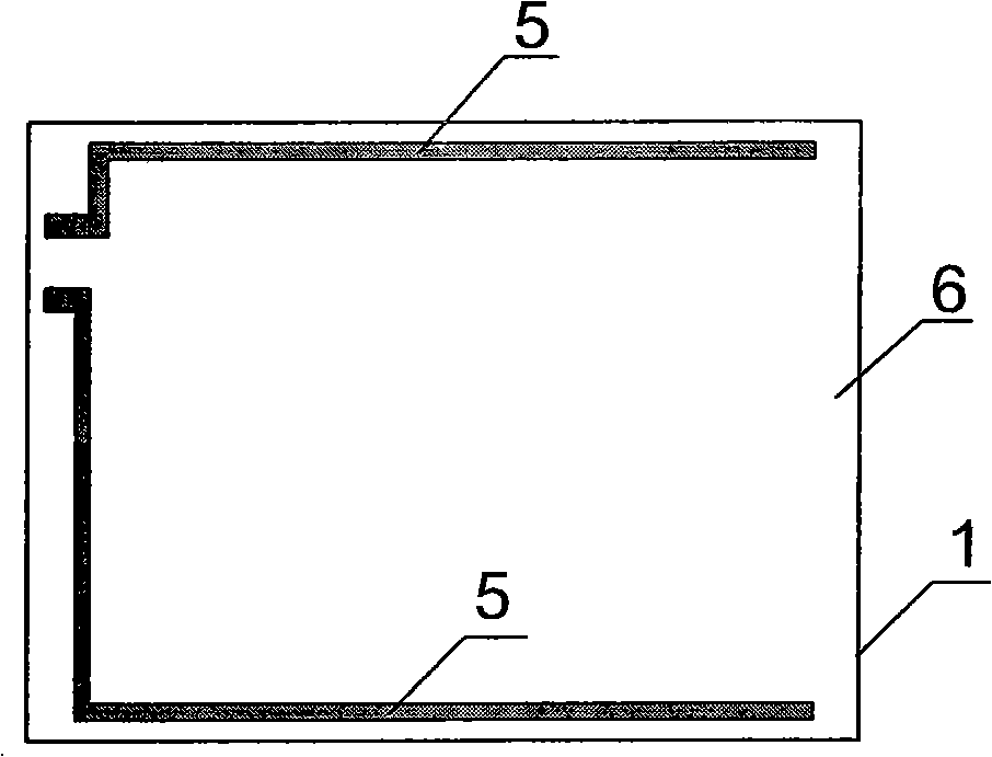
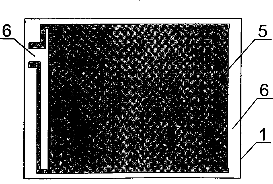
[0031] Pure copper is plated on the resistive layer of transparent conductive film or plate by physical vapor phase; the pure copper plated layer is covered with liquid photosensitive resist or dry film resist, and a resist layer with electrode patterns is formed after exposure and development , or directly print electrode patterns with liquid resist by screen printing; etch pure copper film with alkaline copper chloride etching solution, and finally use a short-wavelength laser less than 1065nm to etch the non-functional area and the isolation line between the electrode and the functional area , after removing the electrode pattern resist film, repeat the same procedure for making the electrode pattern resist film to make a non-functional area pattern resist layer on the resistance layer, and remove the resistance layer in the non-function area with an acidic etching solution.
[0032] Alkaline copper chloride etching solution The etching solution can adopt the formula introdu...
Embodiment 2
[0036] On the resistive layer of transparent conductive film or plate, brass is plated by physical vapor phase; the brass plated layer is covered with liquid photosensitive resist or dry film resist, and a resist layer with electrode patterns is formed after exposure and development. , It is also possible to directly print electrode patterns with liquid resist by screen printing; etch the brass film with alkaline copper chloride etching solution, and finally use a short-wavelength laser less than 1065nm to etch out the isolation lines between the non-functional area and the electrode and functional area , after removing the electrode pattern resist film, repeat the same procedure for making the electrode pattern resist film to make a non-functional area pattern resist layer on the resistance layer, and remove the resistance layer in the non-function area with an acidic etching solution.
Embodiment 3
[0038] On the resistive layer of the transparent conductive film or board, copper is plated in a physical vapor phase; the bronze plated layer is covered with a liquid photosensitive resist or a dry film resist, and a resist layer with electrode patterns is formed after exposure and development. The electrode pattern can be directly printed with liquid resist by screen printing; the bronze film is etched with alkaline copper chloride etching solution, and finally the isolation line between the non-functional area and the electrode and functional area is etched with a short-wavelength laser less than 1065nm. After removing the electrode pattern resist film, repeat the same procedure for making the electrode pattern resist film to form a non-functional area pattern resist layer on the resistance layer, and remove the resistance layer in the non-function area with acid etching solution.
PUM
 Abstract
Description
Claims
Application Information
 - R&D
- Intellectual Property
- Life Sciences
- Materials
- Tech Scout
- Unparalleled Data Quality
- Higher Quality Content
- 60% Fewer Hallucinations
Browse by: Latest US Patents, China's latest patents, Technical Efficacy Thesaurus, Application Domain, Technology Topic, Popular Technical Reports.
© 2025 PatSnap. All rights reserved.Legal|Privacy policy|Modern Slavery Act Transparency Statement|Sitemap|About US| Contact US: help@patsnap.com


