

Method for controlling growing multiple layer film for making multiple-level micro-reflector
A micro-mirror and multi-layer film technology, applied in the field of multi-level micro-mirror production, can solve the problems of difficult to precisely control corrosion or etching depth, difficult to guarantee horizontal accuracy, poor accuracy and repeatability, etc. Repeatability, high level accuracy, high flatness effect
- Summary
- Abstract
- Description
- Claims
- Application Information
AI Technical Summary
Problems solved by technology
Method used
Image

Examples
Embodiment Construction
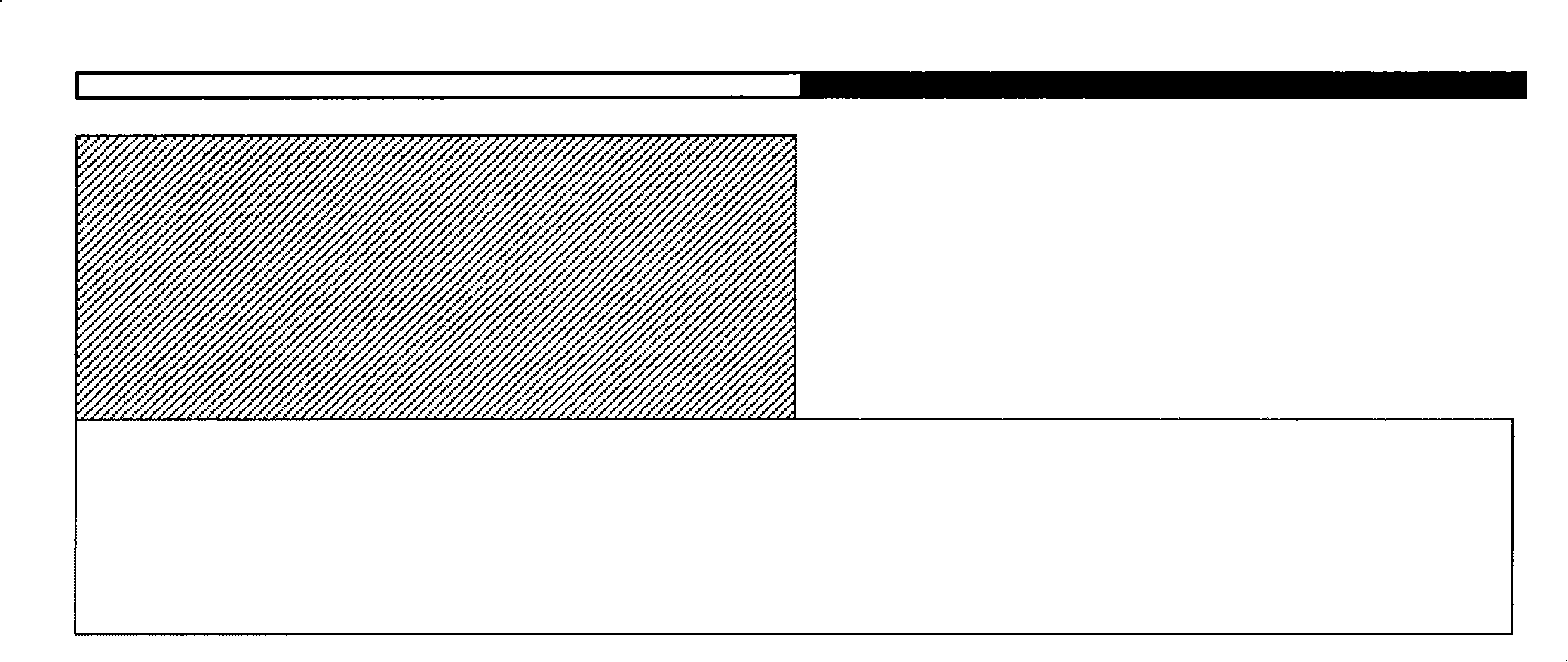
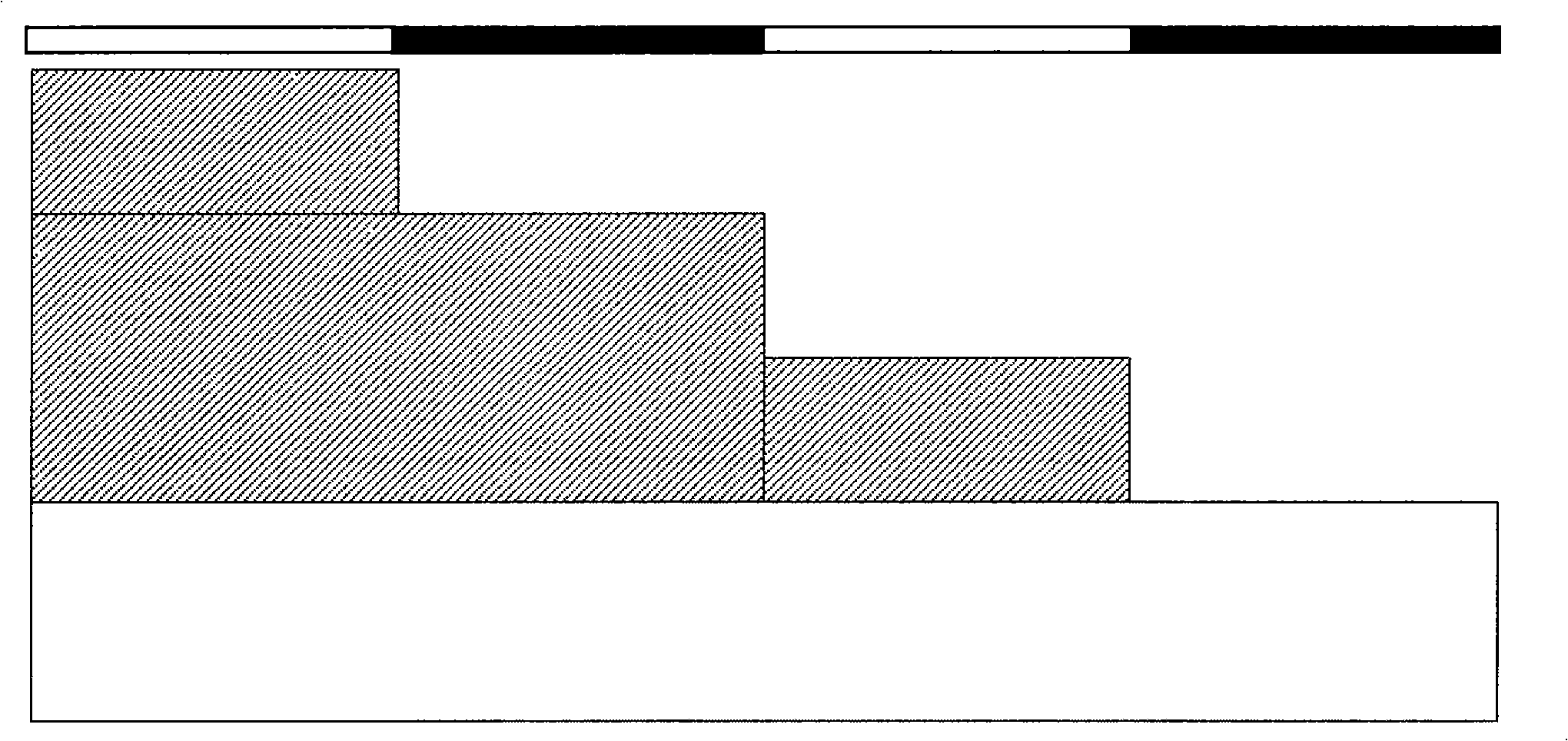
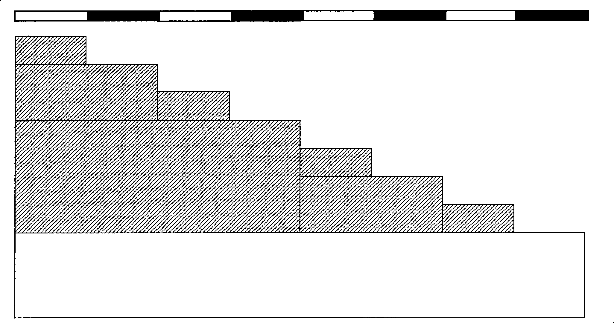
[0022] The method for fabricating a multi-stage micromirror by controlling the growth of multilayer films of the present invention will be described in detail below. This method adopts the controlled growth multilayer film method to make the multistage microreflector, the total number of steps is 16, and the total width of the multistage microreflector is 8mm. The specific process flow is as follows:
[0023] (1) Using double-sided polished silicon or glass or silicon dioxide or silicon carbide or molybdenum sheet or quartz sheet with a surface roughness of 0.2nm to 1μm as the substrate, and cleaning it;
[0024] (2), coat photoresist on the upper surface of the substrate, expose and develop and harden the film with the first photoresist plate to form the required masking pattern; the widths of the bright stripes and dark stripes of the first photoresist plate are respectively L / 2 1 ; and silicon or silicon dioxide or aluminum or gold or copper or silicon carbide or molybdenu...
PUM
| Property | Measurement | Unit |
|---|---|---|
| Surface roughness | aaaaa | aaaaa |
Abstract
Description
Claims
Application Information