Selenide forerunner thin film and method for producing film cell through rapid selenium vulcanizing thermal treatment

A thin-film solar cell and selenide technology, which is applied in the field of compounding, can solve the problems of the difficulty of toxic gas, the low current density of the selenide film, and the influence of the pn junction quality of the thin-film surface structure battery.

Inactive Publication Date: 2008-11-05
NANKAI UNIV +2
View PDF3 Cites 41 Cited by
  • Summary
  • Abstract
  • Description
  • Claims
  • Application Information

AI Technical Summary

Problems solved by technology

The problem is that the deposited film is generally a Cu-rich film, and after heat treatment, it needs to etch or dissolve the Cu in the Cu-rich phase of the film in the KCN solution. 2 Se, which will affect the structure of the film surface and the quality of the pn junction of the battery
The existing problems are: Mo substrate corrodes due to chemical replacement reaction at the initial stage of deposition, the solubility of solute in...

Method used


Image

  • Selenide forerunner thin film and method for producing film cell through rapid selenium vulcanizing thermal treatment
  • Selenide forerunner thin film and method for producing film cell through rapid selenium vulcanizing thermal treatment
  • Selenide forerunner thin film and method for producing film cell through rapid selenium vulcanizing thermal treatment

Examples


Embodiment 1

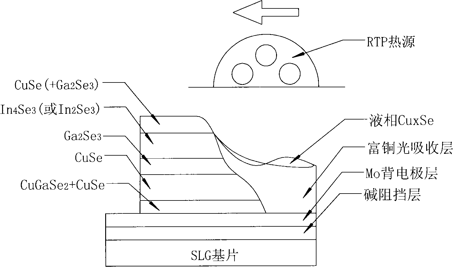
[0039] When making CuInSe with nano-selenide coating 2-x S x For thin-film solar cells, the alkali barrier layer and the Mo back electrode film are sputtered on the surface of the SLG substrate respectively, and the selenide coatings CuSe, In 4 Se 3 (or In 2 Se 3 ) and CuSe each once, the present invention prefers selenium-poor In 4 Se 3 (melting point 520°C) nano-coating; drying immediately after each roll coating, the selenide precursor film presents CuSe / In 4 Se 3 (or In 2 Se 3 ) / CuSe structure, total Cu / In of the film>1.06, CuSe on the surface>CuSe on the bottom, the optimum ratio is 1.1~1.5, and the total thickness after drying is about 4~7μm (the thickness of the absorbing layer prepared after the final rapid selenium vulcanization heat treatment is required to be about 0.9 ~1.8μm), the composition structure ratio of the three-layer selenide film is about 4:10:6.1, before the precursor selenide film is dried for the last time, a certain amount of sodium salt nee...

Embodiment 2

[0045] When making CuIn with nano-selenide coating 0.7 Ga 0.3 Se 2-x S x For thin-film solar cells, four nano-selenide coatings are required, which are: (CuSe+CuGaSe 2 ), Ga 2 Se 3 、In 4 Se 3(or In 2 Se 3 +CuInSe 2 ), CuSe, adjust them to the appropriate viscosity respectively, continuously implement roll coating and drying on the substrate Mo thin film, four kinds of selenide coatings can be continuously formed into films at one time, and its precursor selenide thin film structure is: ( CuSe+CuGaSe 2 ) / Ga 2 Se 3 / In 4 Se 3 (or In 2 Se 3 +CuInSe 2 ) / CuSe, the total Cu / (In+Ga) of the film>1.06, the atomic structure ratio of the four-layer film composition is: (4+4):1:3.5:12.1, the thickness of the precursor selenide film is about 4-7μm, and the film The composition ratio of each element in Ga / (In+Ga)≥0.3, Se / Mbottom CuSe. The feature of this CIGS thin film battery is that the gallium element in the selenide precursor film is concentrated on the bottom layer, ...

Embodiment 3

[0047] Preparation of CuInSe by Electrochemical Deposition of Selenide Precursor Thin Film 2-x S x Thin film solar cells. The ratio of the electrodeposition solution components is: 2.6mMol L -1 CuCl 2 2H 2 O, 9.6mMol L -1 InCl 3 and 5.5mM ol·L -1 h 2 SeO 3 , LiCl0.236Mol L -1 ; And add ph=3 buffer composed of potassium hydrogen phthalate and sulfamic acid to measure the pH~2.6 of the electroplating solution, adopt a three-electrode constant potential system, and the reference electrode is a saturated calomel electrode (SCE). Put the SLG substrate with the alkali barrier layer and the Mo back electrode film deposited by sputtering into the above-mentioned electroplating solution, pre-treat the Mo back electrode film of the substrate at -0.5V for 1 minute, and rinse the substrate with deionized water after taking it out. Blow dry with pure nitrogen, put it aside for a certain period of time, put it into the electroplating solution again for electrodeposition, first pre...


PUM

PropertyMeasurementUnit
Thicknessaaaaaaaaaa

Abstract

The invention relates to a method of a low cost selenide van thin film and the fast selenium sulfuration heat treatment to prepare the solar cell, which can be used in the nm selenide paint roll coating or the electrodeposit method to prepare the selenide van film, through the vacuum flash selenium sulfuration heat treatment, the high efficiency cadmium-free thin film solar cell or the photovoltaic integrated module. The thin film cell adsorption layer band gap is in the v-shaped distribution, and the flash selenium sulfuration heat treatment causes the CuSe in the porous loose thin film fusing, soaking, liquid phase serving the reaction growth of the CIGS film crystal and the self densification of the film with the In4Se3, reactive sputtering In2Se3 or In2S3 to neutralize the excessive CuxSe adsorbed by the film surface layer, going on splashing the micro excessive In2S3 to generate n-high-ohmic resistor Cu(In<1-y>Gay)<3>(SxSe<1-x>)<5> thin film cell shallow burying, then reacting the splashing deposit n-type In(OH,S)/ZnS(O,OH)/Zno(S) buffer layer with the i-layer, linking the slashing transparent conductive film/and laserprocessing collecting ellectrode to complete the preparation of the thin film cell.

Description

technical field [0001] The invention relates to the preparation of compound semiconductor thin film devices, more specifically, to the preparation of copper indium gallium selenide sulfur [Cu(In 0.7 , Ga 0.3 ) Se 2-x S X Abbreviated as CIGS] selenide precursor film of thin film solar cells, and after vacuum rapid selenium sulfide heat treatment, the method of directly and continuously preparing thin film solar cells or photovoltaic integrated modules. Background technique [0002] Solar cell power generation is a renewable energy technology that has the least impact on the environment in the process of generating electricity. For solar power technology to be commercially successful, solar cells must be more efficient, lower cost, better weather-resistant, and not add to other environmental concerns. The development of traditional crystalline silicon solar cell technology benefits from the continuous technological progress of electronic silicon semiconductor materials. To...

Claims


Application Information

Patent Timeline
IPC IPC(8): H01L31/18
CPCY02P70/50
Inventor 孙国忠敖建平杨小锋周志强张超何青刘新路李宝璋
Owner NANKAI UNIV
Why Eureka
Try Eureka