Aligning system, aligning method for photolithography equipment and enhancement type aligning mark

An alignment system and lithography equipment technology, applied in the field of enhanced alignment marks, can solve problems such as line shrinkage, deformation, and limited manufacturing and processing capabilities, so as to improve signal strength, reduce alignment errors, and improve resolution and the effect of alignment accuracy

Active Publication Date: 2008-11-12
SHANGHAI MICRO ELECTRONICS EQUIP (GRP) CO LTD
View PDF3 Cites 27 Cited by
  • Summary
  • Abstract
  • Description
  • Claims
  • Application Information

AI Technical Summary

Problems solved by technology

However, reducing the marking line width or increasing the magnification of the imaging system will bring some problems, such as limited by the resolution of the image sensor and the manufacturing and processing capabilities of the marking, the marking line cannot be reduced indefinitely, and the marking line width The smaller it is, the easier it is to be deformed by the semiconductor process

Method used


Image

  • Aligning system, aligning method for photolithography equipment and enhancement type aligning mark
  • Aligning system, aligning method for photolithography equipment and enhancement type aligning mark
  • Aligning system, aligning method for photolithography equipment and enhancement type aligning mark

Examples


Embodiment Construction

[0073] The specific implementation manners of the present invention will be further described in detail below in conjunction with the accompanying drawings.

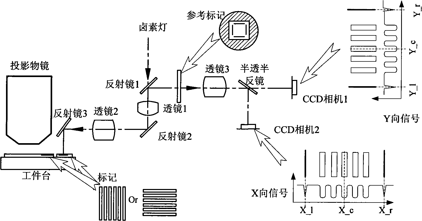
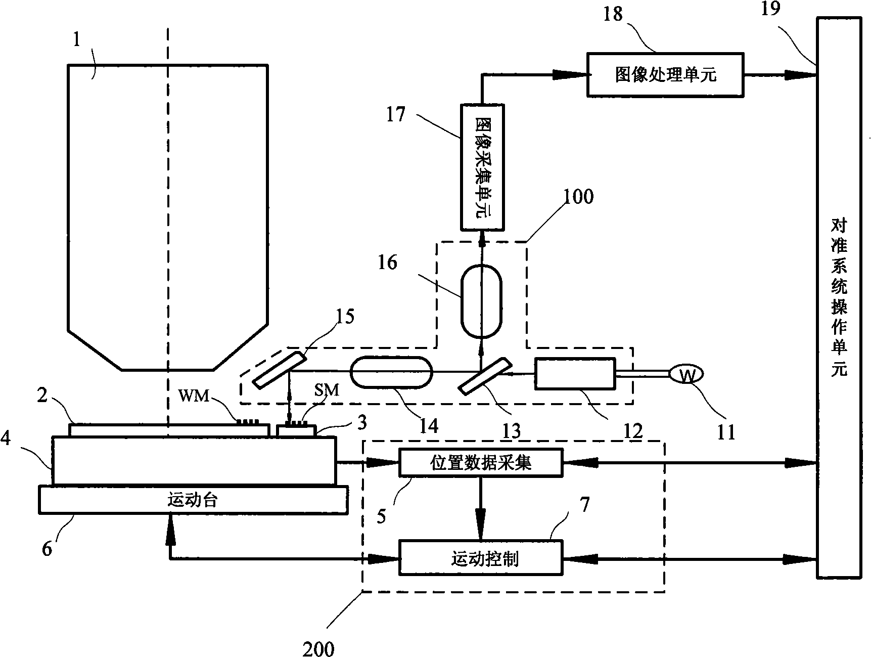
[0074] figure 2 A structural schematic diagram of an embodiment provided by the present invention, the alignment system is used to establish the coordinate position relationship between the silicon wafer alignment mark WM and the reference plate mark SM, that is, to realize the alignment between the silicon wafer and the reference plate, It includes: an alignment mark WM on the silicon wafer 2 and an alignment mark SM on the reference plate 3, a light source module 11, an illumination and imaging unit 100, an image acquisition unit 17, an image processing unit 18, an alignment An operation unit 19, and a position acquisition and motion control unit 200.

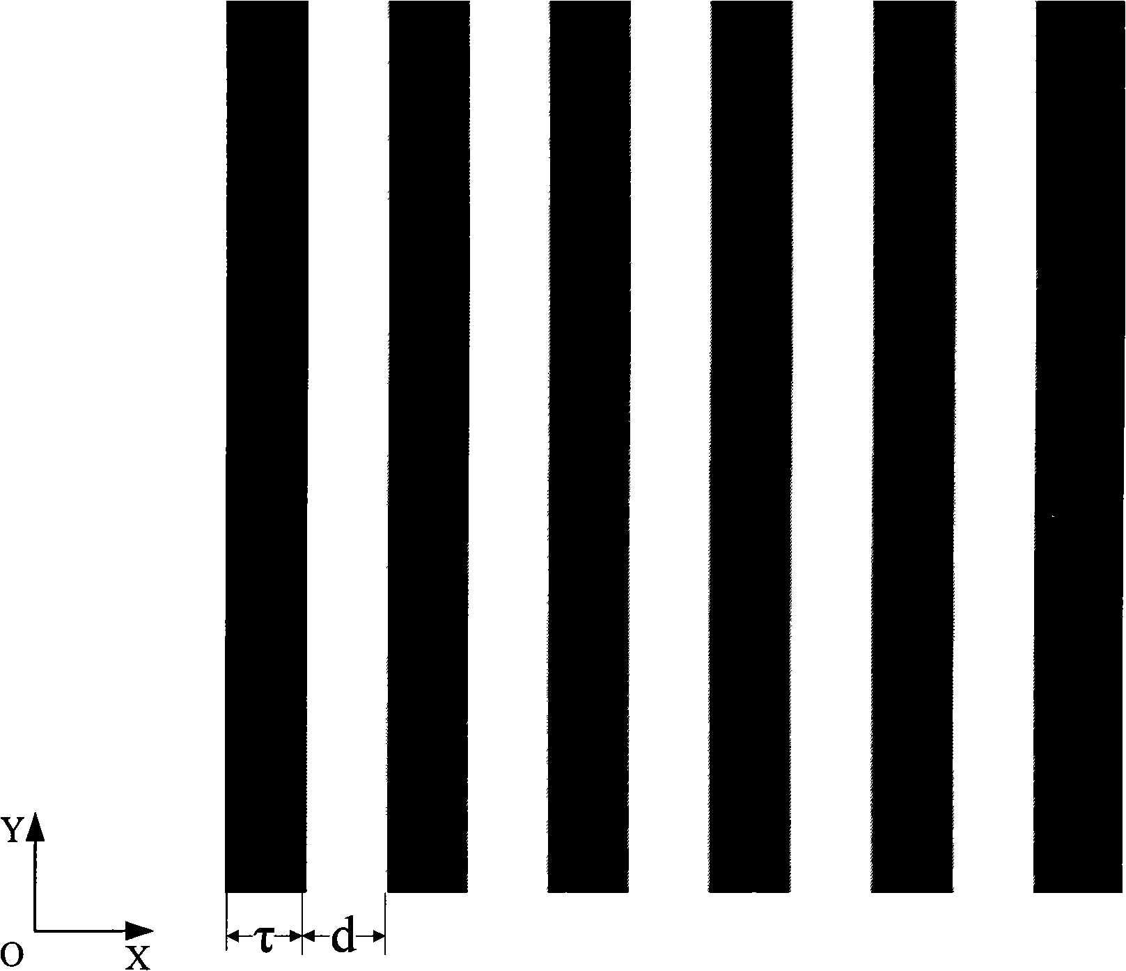
[0075] The wafer mark WM or the reference plate mark SM is composed of a group of equidistant lines, wherein the width of the lines is equal to the width of the groov...


PUM

PropertyMeasurementUnit
wavelengthaaaaaaaaaa

Abstract

The invention provides an alignment system, an alignment method and an enhanced alignment mark for lithography equipment. By taking advantage of a designed special alignment mark structure, the image signal of the alignment mark can be obtained through an alignment imaging system; through Fourier transformation, the image signal of the alignment mark is conversed to a frequency space so as to extract the frequency information of the marks in different levels; and through Fourier inverse transformation, the alignment signals of each corresponding frequency level are obtained, and contain the inner structure and phase information of the alignment marks; at last, the coarse alignment is carried out through original signals or obtained low level frequency; by making use of the alignment signals of high level frequency to do precision alignment, alignment resolution and precision are enhanced. Moreover, the invention also provides two types of enhanced alignment marks to enhance the signal strength of frequency component in special level, increases the signal-to-noise ratio of the signal of the level and reduces alignment error.

Description

technical field [0001] The invention relates to photolithographic devices in the field of integrated circuit or other micro-device manufacturing, in particular to an alignment system, an alignment method and enhanced alignment marks for photolithographic equipment. Background technique [0002] In the manufacturing process of semiconductor IC integrated circuits, a complete chip usually needs to undergo multiple photolithography exposures before it can be completed. Except for the first photolithography, the photolithography of other levels must be precisely positioned before exposure, so as to ensure the correct relative position between the two layers of graphics, that is, overlay accuracy. Overlay accuracy is one of the key technical indicators of projection lithography machines. There are many factors affecting the overlay accuracy, among which the alignment accuracy between the mask and the silicon wafer is one of the important influencing factors. [0003] The early...

Claims


Application Information

Patent Timeline
Patent Type & Authority Applications(China)
IPC IPC(8): G03F7/20G03F9/00
Inventor 李运锋韦学志徐荣伟宋海军
Owner SHANGHAI MICRO ELECTRONICS EQUIP (GRP) CO LTD
Why Eureka
Try Eureka