Method and device for forming PN junction on P type mercury cadmium telluride by laser process

A laser processing and mercury cadmium telluride technology, which is applied in laser welding equipment, metal processing equipment, manufacturing tools, etc., can solve the problems of increasing the probability of blind cells in photosensitive element arrays and the negative impact on device yield, so as to reduce the blind cell rate , The effect of simple knot formation process

Inactive Publication Date: 2008-12-03
SHANGHAI UNIV
View PDF0 Cites 12 Cited by
  • Summary
  • Abstract
  • Description
  • Claims
  • Application Information

AI Technical Summary

Problems solved by technology

In these traditional methods, photolithography is an indispensable process step, and a series of physical and chemical processes such as photolithography coating, development, and degumming will increase the probability of blind cells in the photosensitive element array, thereby affecting the quality of the device. rate negatively affects

Method used


Image

  • Method and device for forming PN junction on P type mercury cadmium telluride by laser process
  • Method and device for forming PN junction on P type mercury cadmium telluride by laser process
  • Method and device for forming PN junction on P type mercury cadmium telluride by laser process

Examples


Embodiment Construction

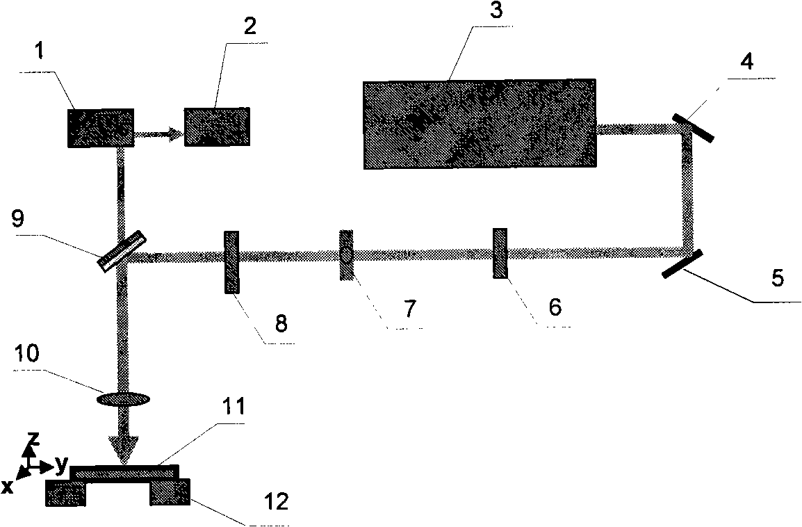
[0018] A preferred embodiment of the present invention is described in detail as follows in conjunction with accompanying drawing:

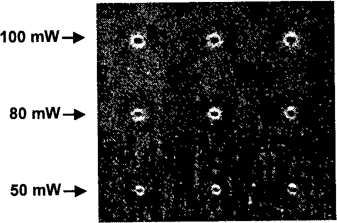
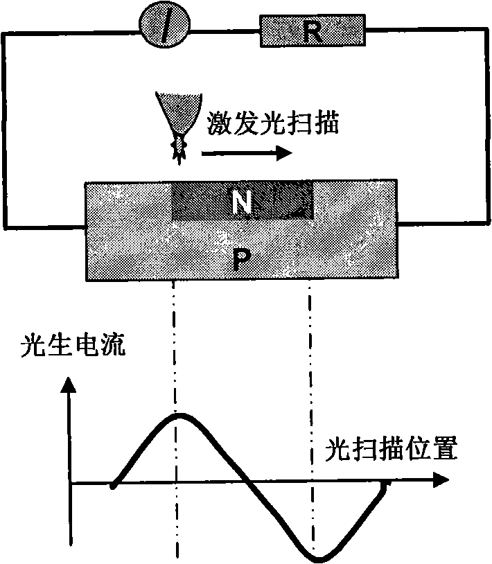
[0019] The method of laser processing in this example to form a PN junction on the P-type HgCdTe material is: focus the pulse laser on the surface of the P-type HgCdTe material, and irradiate the P-type HgCdTe material in a short period of time. In this way, a hole area ablated by the laser is formed on the material, and the diameter of the hole is several microns to more than ten microns; an inversion area, that is, an N-type area, is formed in the area of ​​several microns around the hole, and the inversion area and the P area around the hole are formed. Type region forms a PN junction region.

[0020] The experimental sample in this example is a HgCdTe film material grown on a CdZnTe substrate by liquid phase epitaxy. The thickness of the epitaxial film is 24 μm, and the surface is covered with a 0.25 μm ZnS passivation layer. Hall test gives...


PUM

PropertyMeasurementUnit
thicknessaaaaaaaaaa
diameteraaaaaaaaaa

Abstract

The invention relates to a laser processing method for forming a PN-junction on a P-typed Hg-Cd-Te material and a device thereof. The method comprises the following steps that: a pulse laser is focused on the surface of the P-typed Hg-Cd-Te material and the P-typed Hg-Cd-Te material is radiated in short time, thus forming a porous area melted and corroded on the material by the laser; the diameter of the pore is within a range from several micrometers to ten micrometers or so; an inversion area, namely an N-typed area is formed in the several micrometer area around the pore; the inversion area and the P-typed area at the periphery of the pore form a PN-junction area. The device of the invention consists of a femto-second laser, a deflecting mirror, a neutral density filter, a pupil, an aperture, a dichroic mirror, a lens, a CCD camera, a display and a workpiece platform. As the method of the invention has the advantages of laser direct writing, saves the lithography process step in the traditional junction-forming technique, leads the junction-forming process to be simplified and is beneficial to reducing the dead pixel caused by the process complexity. The method of the invention is completely compatible with other techniques of the prior art in the field such as read-out circuit technique and has direct and practical value.

Description

technical field [0001] The invention relates to a method and a device for forming a PN junction on a P-type mercury cadmium telluride material by laser processing, and belongs to the field of infrared photodetectors based on narrow band gap semiconductor mercury cadmium telluride materials. Background technique [0002] For a long time, mercury cadmium telluride (HgCdTe) has been widely used as a very important infrared photodetector material in military infrared thermal imaging, aerospace and satellite infrared remote sensing [Tang Dingyuan, Tong Peiming, Narrow Bandgap Semiconductor Infrared Detector , Semiconductor Devices and Research Progress II, Science Press, 1991]. In particular, photodiode array devices based on HgCdTe materials-infrared focal plane devices (including micromechanical scanning linear devices or staring focal plane devices) are currently one of the mainstream developments in the field of infrared detectors in the world [A .Rogalski, Infrared Detector...

Claims


Application Information

Patent Timeline
Patent Type & Authority Applications(China)
IPC IPC(8): H01L31/18B23K26/04B23K26/38B23K26/382
Inventor 查访星马洪良
Owner SHANGHAI UNIV
Why Eureka
Try Eureka