Patterned hard mask layer preparation method, capacitor array structure and preparation method thereof

A hard mask layer, hard mask technology, applied in the direction of electrical solid devices, circuits, electrical components, etc., can solve the problems of electrical connection and isolation, affecting memory performance, component size reduction, etc. Reduced misalignment issues, good functional effects

Active Publication Date: 2022-03-15
CHANGXIN MEMORY TECH INC
View PDF6 Cites 0 Cited by
  • Summary
  • Abstract
  • Description
  • Claims
  • Application Information

AI Technical Summary

Problems solved by technology

[0004] In the prior art, the multi-pass photolithography process prepares and forms the capacitance hole of the capacitor, so that there is a problem of misalignment of the photomask in the photolithography process, which will affect the electrical connection and isolation between the components in the memory. The performance of the subsequently formed memory, and also detrimental to achieving component size reduction

Method used


Image

  • Patterned hard mask layer preparation method, capacitor array structure and preparation method thereof
  • Patterned hard mask layer preparation method, capacitor array structure and preparation method thereof
  • Patterned hard mask layer preparation method, capacitor array structure and preparation method thereof

Examples


Embodiment 1

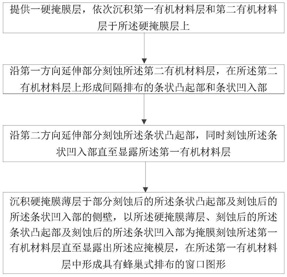
[0115] This embodiment provides a method for preparing a patterned hard mask layer. Such as figure 1 As shown, the method of the present embodiment includes the following steps:

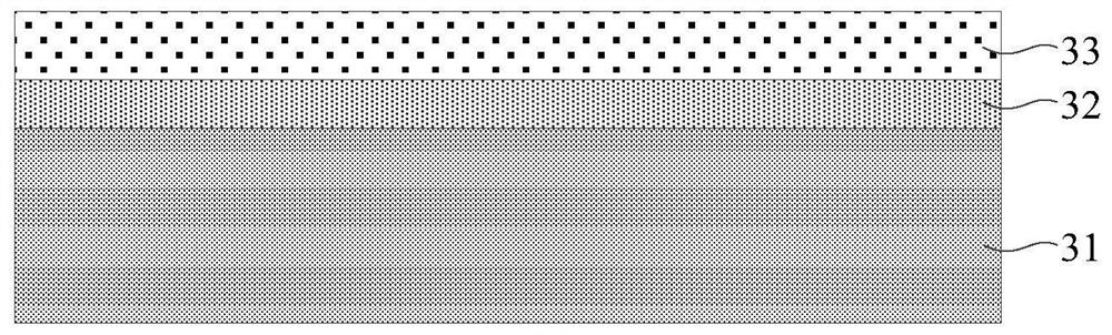
[0116] providing a hard mask layer, sequentially depositing a first organic material layer and a second organic material layer on the hard mask layer;

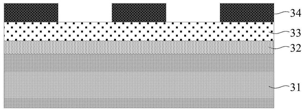
[0117] Etching the second organic material layer along a portion extending along the first direction, forming strip-shaped protrusions and strip-shaped recesses arranged at intervals on the second organic material layer;

[0118] Etching the strip-shaped protrusion part along the second direction, and etching the strip-shaped concave part at the same time until the first organic material layer is exposed;

[0119] Depositing a hard mask thin layer on the partially etched strip-shaped protrusions and the sidewalls of the etched strip-shaped concave portions, using the hard mask thin layer and the etched strips The strip-shaped convex portion and th...

Embodiment 2

[0140] This embodiment provides a method for preparing a capacitor array structure, such as Figure 28 As shown, the method of the present embodiment includes the following steps:

[0141] A semiconductor substrate is provided, the semiconductor substrate includes a plurality of capacitive contact nodes located in the memory array structure, the first and second sacrificial layers, the middle supporting layer, the third sacrificial layer and the upper supporting layer are sequentially formed on the semiconductor substrate layer, and depositing a barrier layer over the second support layer;

[0142] A patterned hard mask layer with windows arranged in a honeycomb arrangement is formed on the above structure, and based on the patterned hard mask layer, the barrier layer, the second supporting layer, the second sacrificial layer, the first The support layer and the first sacrificial layer are used to form a capacitor hole corresponding to the window, and the capacitor hole expos...

Embodiment 3

[0151] This embodiment also provides a method for preparing a capacitor array structure. The similarities between this embodiment and Embodiment 2 will not be repeated, and the difference lies in:

[0152] The method described in this embodiment also includes, as Figure 32 As shown, conductive material is deposited on the bottom and sidewall of the capacitor hole 20 to form the capacitor bottom electrode 10 , and then the first sacrificial layer 22 , the second sacrificial layer 23 , the third sacrificial layer 25 and the barrier layer 27 are removed. Then, if Figure 33 As shown, a capacitor dielectric layer 11 is deposited and formed on the inner surface of the capacitor lower electrode 10 and the exposed outer surface, an upper electrode inner lining layer 12 is formed on the surface of the capacitor dielectric layer 11, and an upper electrode inner lining layer 12 is formed on the surface of the upper electrode inner lining layer 12. The hole-filling body 13 for the uppe...


PUM

PropertyMeasurementUnit
thicknessaaaaaaaaaa
thicknessaaaaaaaaaa
thicknessaaaaaaaaaa

Abstract

The invention provides a method for preparing a patterned hard mask layer, a capacitor array structure and a method for preparing the same. A hard mask layer is provided, and a first organic material layer and a second organic material layer are sequentially deposited thereon, and the second organic material layer is partially etched along the first direction and the second direction; and then the hard mask layer is deposited layer on the sidewall of the etched second organic material layer, use the etched second organic material layer and the hard mask thin layer as a mask to etch the first organic material layer until the hard mask layer is exposed, and A pattern of windows arranged in a honeycomb arrangement is formed on the first organic material layer. The technical solution of the invention significantly increases the density of capacitor holes, so more capacitors can be provided under the same size. For the same number of capacitors, the size of the chip in the present invention is smaller, which is beneficial to realize the reduction of device size.

Description

technical field [0001] The invention relates to the technical field of semiconductor integrated circuit manufacturing, in particular to a method for preparing a patterned hard mask layer, a capacitor array structure and a method for preparing the same. Background technique [0002] As one of the necessary components in integrated circuits, capacitors have functions such as voltage adjustment and filtering in circuits, and are widely used in integrated circuits. In the Dynamic Random Access Memory (DRAM for short) process below 20nm, the DRAM adopts a stacked capacitor structure, and its capacitor (Capacitor) is in the shape of a vertical cylinder with a high aspect ratio. Vertical capacitors form deep grooves in the substrate, and use the sidewalls of the deep grooves to provide the main plate area, thereby reducing the area occupied by the capacitor on the chip surface, while still obtaining a large capacitance. [0003] However, as the chip size continues to decrease, the...

Claims


Application Information

Patent Timeline
Patent Type & Authority Patents(China)
IPC IPC(8): H01L21/027H01L21/8242H01L27/108
CPCH01L21/0274H10B12/30H10B12/03
Inventor 不公告发明人
Owner CHANGXIN MEMORY TECH INC
Why Eureka
Try Eureka