A kind of preparation method of phase-change memory array

A phase-change memory and phase-change storage technology, which is applied in the field of micro-nano electronics, can solve the problems of lengthy process, complex process, and increasing the number of three-dimensional stacking layers, and achieve the goals of improving the preparation process, simplifying the preparation process, and saving photolithography stripping steps Effect

Active Publication Date: 2022-02-11
HUAZHONG UNIV OF SCI & TECH
View PDF6 Cites 0 Cited by
  • Summary
  • Abstract
  • Description
  • Claims
  • Application Information

AI Technical Summary

Problems solved by technology

This technology can theoretically be stacked infinitely, but the current mainstream preparation method has a lengthy process and complicated process. If the preparation process of two-dimensional planar single-layer devices is simplified, the preparation process of three-dimensional memory devices can be greatly improved and the success of the process can be improved. rate, and even increase the number of layers of 3D stacking

Method used


Image

  • A kind of preparation method of phase-change memory array
  • A kind of preparation method of phase-change memory array
  • A kind of preparation method of phase-change memory array

Examples


preparation example Construction

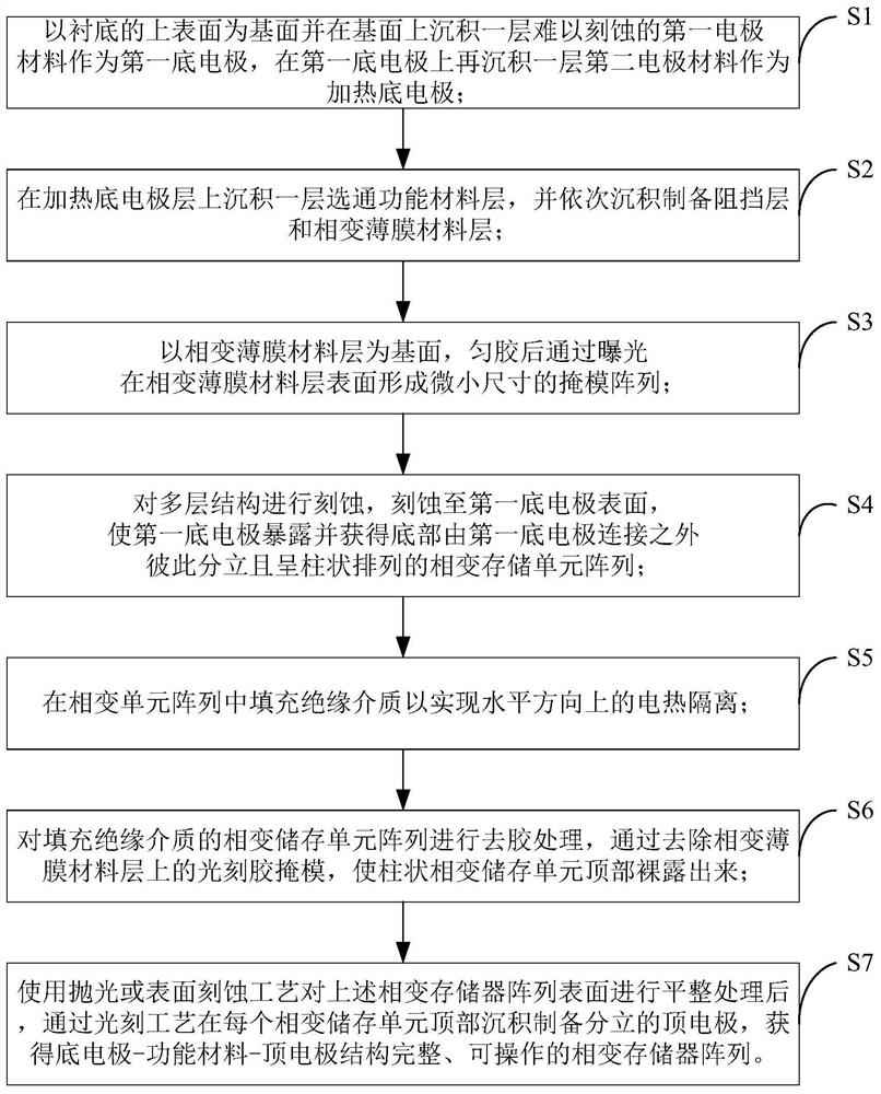
[0047] The present invention provides a method of preparing a phase change memory array. Compared to the conventional process, the present invention adopts the idea of ​​the overall etching of the multilayer film, and does not require each layer to add a photolithography process. The patterning is realized, but the overall pattern etching is performed after the end of the multilayer structure deposition, which can reduce the photolithography step, reduce production cost, improve productivity and yield.

[0048] like figure 1 As shown, the present invention provides a phase change memory array integral preparation process, and specifically includes the following steps:

[0049] S1: The upper surface of the substrate is the base surface, and a layer of first electrode material is deposited on the base surface as a first bottom electrode, and a layer of second electrode material is deposited on the first bottom electrode as a heating electrode; The first bottom electrode material is ...

Embodiment 1

[0065] This Example 1 includes the following steps:

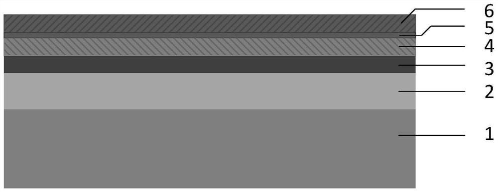
[0066] Step 1: There are SIOs on the surface 2 On the single crystal silicon substrate 1 of the insulating layer, 200 nm Pt is deposited by a magnetron sputtering process as a first bottom electrode 2.

[0067] Step 2: On the basis of step one, 100 nm W is deposited by the magnetron sputtering process as the heating bottom electrode 3.

[0068] Step 3: On the basis of step two, 100 nm gese is deposited by the magnetron sputtering process as the strobe function material layer 4.

[0069] Step 4: On the basis of step three, 10 nm W is deposited by the magnetron sputtering process as the barrier layer 5.

[0070] Step 5: On the basis of step four, 100 nm GE is deposited by magnetron sputtering process. 2 SB 2 TE 5 As the phase change film material layer 6, such as figure 2 Indicated.

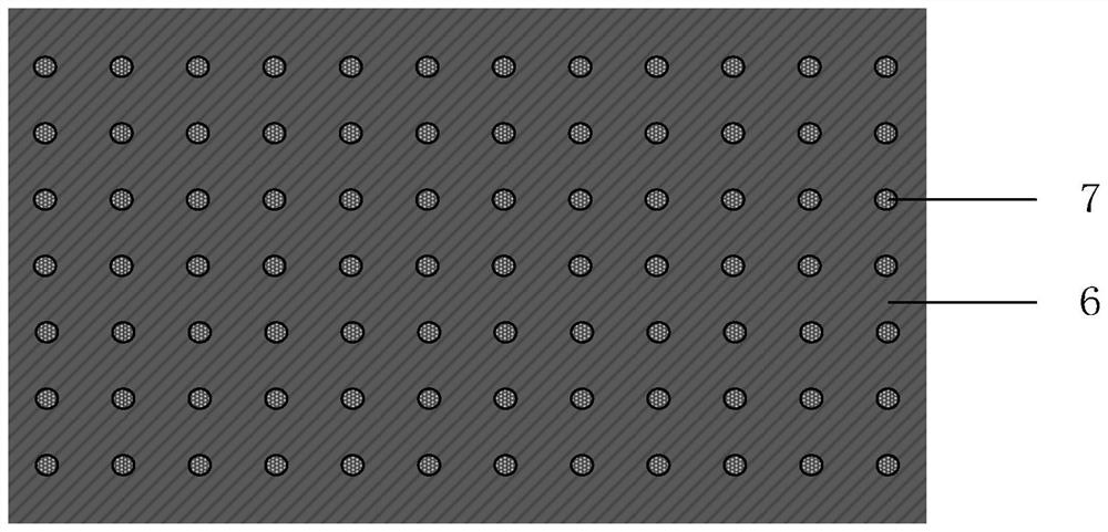
[0071] Step 6: On the basis of step five, a uniform photoresist 7 is applied to the layer of the phase change film material using a hierarch.

[00...

Embodiment 2

[0080] This Example 2 includes the following steps:

[0081] Step 1: There are SIOs on the surface 2 On the single crystal silicon substrate of the insulating layer, 200 nm Pt is deposited by a magnetron sputtering process as a first bottom electrode.

[0082] Step 2: On the basis of step one, 100 nm W is deposited by the magnetron sputtering process as the heating electrode.

[0083] Step 3: On the basis of step two, 100 nm GE is deposited by magnetron sputtering process. 2 SB 2 TE 5 As the phase change film material, such as Figure 8 Indicated.

[0084] Step 4: On the basis of step three, the hierarch is used to spin a uniform photoresist on the phase change film material layer.

[0085] Step 5: On the basis of step four, a circular mask array of small sizes is formed on the surface of the phase change film material using electron beam exposure, such as Figure 9 Indicated.

[0086] Step Six: Erregate the multilayer film structure by ICP etching equipment until the first bottom e...


PUM

PropertyMeasurementUnit
thicknessaaaaaaaaaa
thicknessaaaaaaaaaa
sizeaaaaaaaaaa

Abstract

The invention belongs to the technical field of microelectronic devices and memory, and discloses a preparation method of a phase change memory array, which specifically includes: depositing a multilayer film structure on a substrate, including a bottom electrode layer, a heating electrode layer, and a gate material layer , connection barrier layer, phase change functional layer. After the thin film is prepared, only one photolithography process is used to pattern the entire part above the bottom electrode, and then it is etched to fill the electric and thermal isolation insulating layer between the units, and a separate top electrode is prepared through an additional photolithography process to obtain the bottom electrode- Functional Materials - Top Electrode Structurally Complete and Operable Phase Change Memory Arrays. The reduction in the number of photolithography processes in the process can not only reduce the cost in the production process, but also improve production efficiency and yield. At the same time, the simplification of the preparation process of two-dimensional planar single-layer devices can greatly improve the preparation process of three-dimensional memory devices. Therefore, a three-dimensional memory technology in which two-dimensional planar single-layer memories are stacked in multiple layers in the vertical direction is realized.

Description

Technical field [0001] The present invention belongs to the field of micro-nano-electronic technology, and more relates to a data memory, and more particularly to a method of preparing a phase change memory array. Background technique [0002] In today's electronic technology and the rapid development of the information industry, as data is explosive, people's demand for non-volatile memory is increasing. The phase change memory (PCM) has the advantages of high integration, fast response speed, long and low power consumption, and so on by the International Semiconductor Industry Association to become the future mainstream reservoir. [0003] The basic principle of the phase change memory cell is to use the electrical pulse signal to the device unit, so that the phase change thin film material can be retrofitable between amorphous and polysone to achieve "0" and "1" storage. A narrow pulse width, high-value electrical pulse is applied to the RESET operation, and the crystalline-st...

Claims


Application Information

Patent Timeline
Patent Type & Authority Patents(China)
IPC IPC(8): H01L45/00
CPCH10N70/231H10N70/061H10N70/826
Inventor 程晓敏曾运韬童浩缪向水
Owner HUAZHONG UNIV OF SCI & TECH
Why Eureka
Try Eureka