
Method for preparing heat sink composite material for semiconductor substrate

A composite material and semiconductor technology, applied in the field of preparation of semiconductor substrate heat sink composite materials, can solve the problems of small friction coefficient, unfavorable thermal conductivity of materials, and reduced polishing strength, etc.

Inactive Publication Date: 2008-12-17
SHANGHAI UNIV
View PDF0 Cites 14 Cited by
  • Summary
  • Abstract
  • Description
  • Claims
  • Application Information

AI Technical Summary

Problems solved by technology

However, the surface hardness of the diamond film is very high, and it takes time and effort to polish it.
However, compared with conventional micro-diamond films, nano-diamond film grains can be as small as several nanometers, so its surface is smooth and its coefficient of friction is small. At the same time, its hardness is about 10-20% lower than conventional diamond, greatly Reduced its polishing strength
[0007] But on the other hand, the nanoscale grain size of the nanodiamond film is an unfavorable factor for the thermal conductivity of the material

Method used


Image

  • Method for preparing heat sink composite material for semiconductor substrate

Examples


Embodiment 1

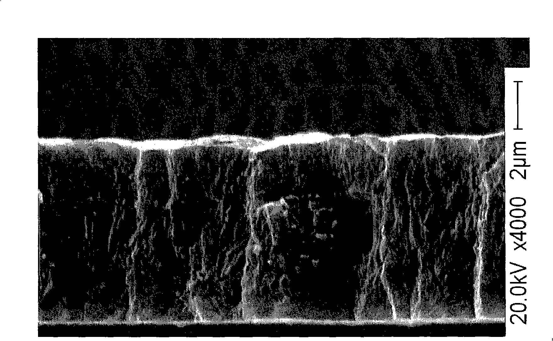
[0020] In this embodiment, a diamond film is prepared by a hot filament chemical vapor deposition (HFCVD) method. The HFCVD method is the most commonly used method for preparing diamond thin films. It has the advantages of simple equipment, fast growth speed, good quality, and easy realization of large-area deposition. The specific process and steps are as follows:

[0021] (1) Tantalum wire pretreatment: Polish the surface of the tantalum wire with sand, evacuate to 3Pa, then pass hydrogen and acetone to 5kPa, where the ratio of hydrogen to acetone is 2:1, heat to 450 ° C for 30 minute.

[0022] (2) Silicon substrate pretreatment: In the experiment, the growth of the diamond film is based on a P-type silicon wafer (with a resistivity of about several Ω cm) with an area of ​​1cm×1cm, and its mirror surface is used as the diamond growth surface. The purpose is to In order to reduce the roughness of the diamond surface. First place the silicon substrate in HF solution for 10 ...


PUM

PropertyMeasurementUnit
particle sizeaaaaaaaaaa
surface roughnessaaaaaaaaaa

Abstract

The invention relates to a preparation method of a semiconductor substrate heat sink composite material, which mainly comprises the steps of pre-treating a tantalum wire, pre-treating a silicon substrate, placing a pretreated silicon wafer into a reaction chamber of a hot wire chemical vapor deposition device to be used as a deposition substrate; vacuuming, introducing reactants hydrogen gas and acetone, and allowing nucleation of a microcrystalline diamond film; adjusting the flow rate, temperature and other conditions of the acetone and the hydrogen gas, and allowing growth of the microcrystalline diamond film; allowing growth of a nano-crystal diamond film; and adjusting the flow rate of the acetone and the hydrogen gas, controlling the substrate temperature at 600-650 DEG C, and allowing the film to grow for 3-5 hours to obtain a diamond composite film with a relatively smooth surface, i.e. the semiconductor substrate heat sink composite material. The inventive semiconductor substrate heat sink composite material has the advantages of simple equipment, rapid growth speed, good quality, easy implementation of large area deposition, etc.

Description

technical field [0001] The invention relates to a method for preparing a semiconductor substrate heat sink composite material, and belongs to the technical field of manufacturing technology of inorganic non-metallic material devices. Background technique [0002] For a long time, the development of silicon technology in the semiconductor industry has followed Moore's law, and the number of transistors on an integrated chip increases exponentially with time. However, this momentum will be hampered by material performance limitations, the biggest of which is heat dissipation. ITRS (International Technology Roadmap for Semiconductors) predicts that between 2005 and 2009, the maximum junction temperature of high-power chips will reach 85°C. [0003] The SOI (silicon on insulator) technology that is widely used in the integrated circuit industry is developed instead of the original CMOS technology. The only advantage SOI has over bulk silicon is that silicon dioxide provides el...

Claims


Application Information

Patent Timeline
Patent Type & Authority Applications(China)
IPC IPC(8): H01L21/02H01L21/31C23C16/27
Inventor 王林军管玉兰黄健戴文琦夏义本
Owner SHANGHAI UNIV
Learn More