
Nitrogen-silicon congruent melting alloy, method for manufacturing same and use

A eutectic and alloying technology, applied in chemical instruments and methods, self-melting liquid pulling method, crystal growth, etc., can solve the problems of fluctuation of silicon nitride formation amount, large weighing error, and small amount of doping.

Active Publication Date: 2009-01-07
GRINM SEMICONDUCTOR MATERIALS CO LTD
View PDF0 Cites 3 Cited by
  • Summary
  • Abstract
  • Description
  • Claims
  • Application Information

AI Technical Summary

Problems solved by technology

The disadvantages of this method are: nitrogen can form particles above the silicon melt, and when they fall, they can destroy the growth of single crystals; in addition, it takes a long time for silicon nitride to be fully melted; Mass flow meter, the amount of silicon nitride formed on the surface of molten silicon also fluctuates greatly, causing the quality fluctuation of nitrogen in the grown single crystal
The direct doping method has two disadvantages: one is that the amount of doping is too small, and the weighing error is large; the other is that silicon nitride is very stable in molten silicon, and it takes a long time to be fully melted.

Method used


Image

  • Nitrogen-silicon congruent melting alloy, method for manufacturing same and use
  • Nitrogen-silicon congruent melting alloy, method for manufacturing same and use
  • Nitrogen-silicon congruent melting alloy, method for manufacturing same and use

Examples


Embodiment 1

[0020] In a quartz crucible with a diameter of 356 mm, 1 gram of silicon nitride and 45,000 grams of polysilicon were respectively added. After the melting was completed, the polysilicon was cooled, and the nitrogen concentration in the polysilicon was measured by sampling to be 7E17 atoms / cm3.

Embodiment 2

[0022] In a quartz crucible with a diameter of 254 mm, 24 mg and 10,000 grams of silicon nitride and polysilicon were added respectively. After melting, the polysilicon was cooled, and the nitrogen concentration in the polysilicon was measured by sampling to be 7E16 atoms / cm3.

Embodiment 3

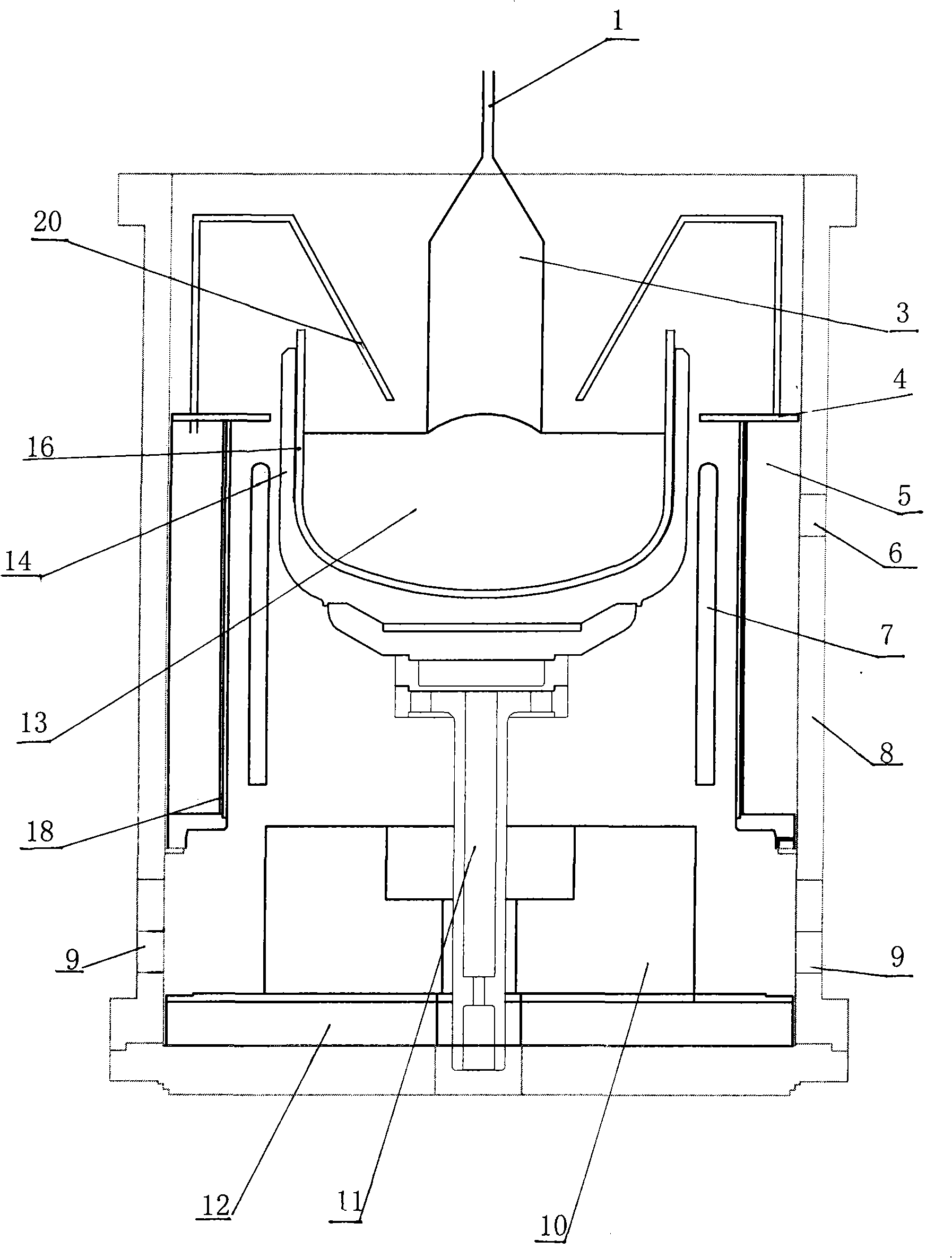
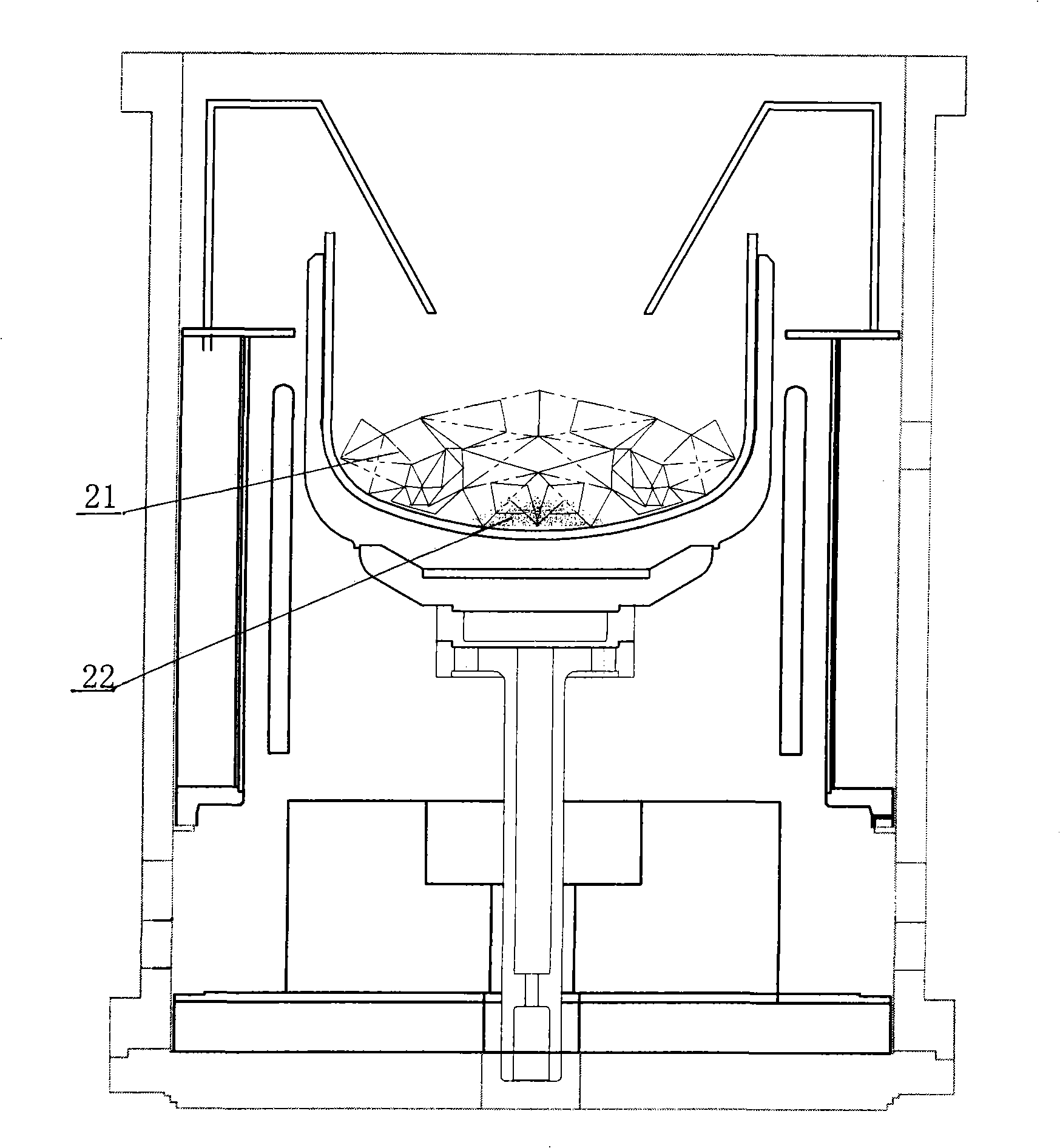
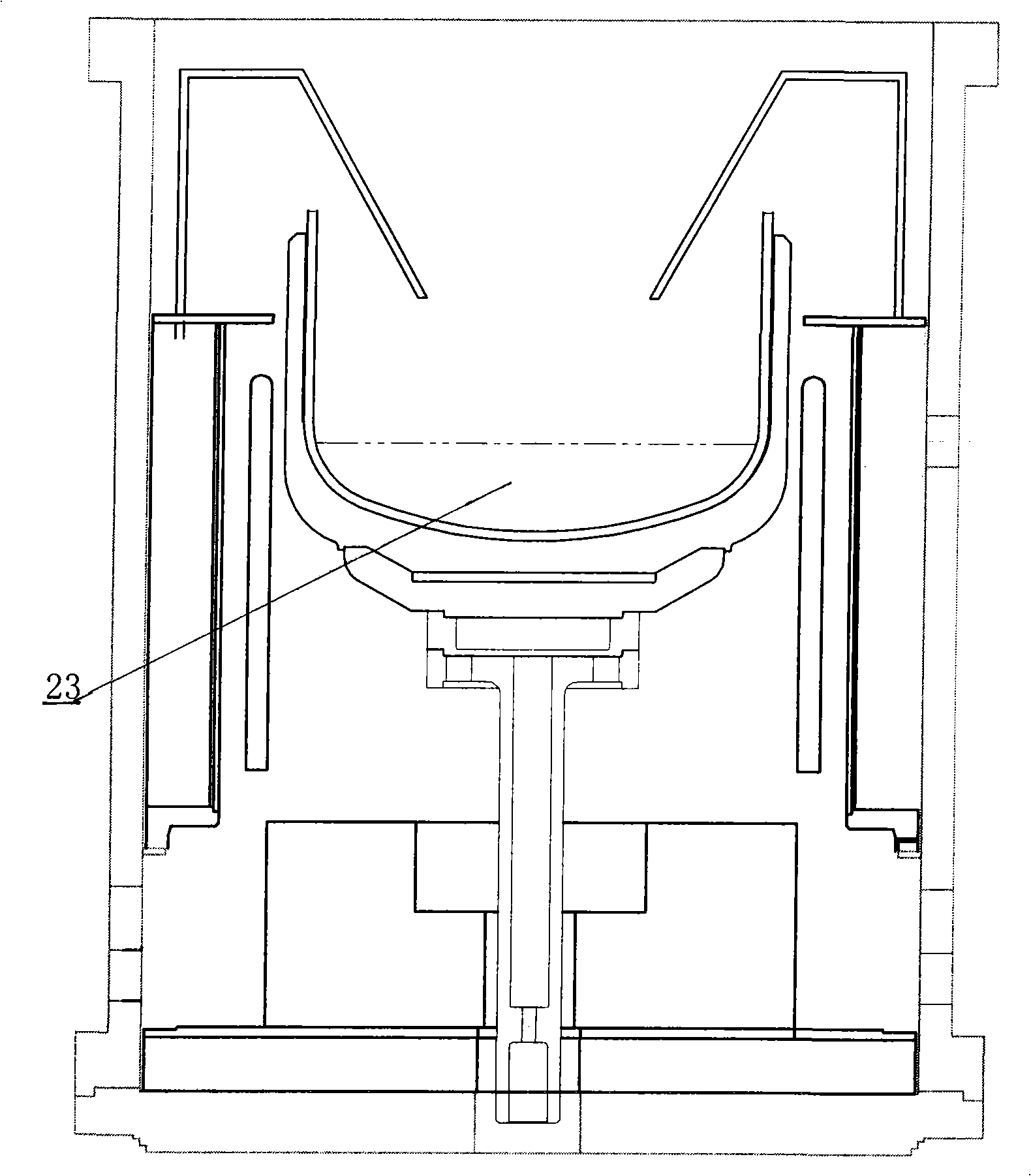
[0024] The specific manufacturing method of silicon nitride eutectic alloy is described as follows: on the thermal field used for crystal pulling, first put the quartz crucible into the graphite crucible, put a certain amount of silicon nitride powder on the bottom of the quartz crucible, and then add For polysilicon, argon gas is introduced, and pumping is used at the same time to keep the pressure inside the furnace at 4-50 torr, and the power is increased to melt the polysilicon until it is completely melted, and the heating power is maintained until the silicon nitride powder is completely melted. Then reduce the heating power to 0 in 1-10 times, and after cooling for several hours, take out the polysilicon at the bottom of the crucible together with the adhered quartz. The quartz is then removed with hydrofluoric acid. Take the polycrystalline block to measure the nitrogen content inside. This polysilicon is then broken and cleaned. This is the nitrogen-containing polys...


PUM


Abstract

The invention relates to silicon nitride eutectic and a manufacturing method and an application thereof. Total nitrogen concentration in the silicon nitride eutectic is 1E16 to 7E18 atom / ccm. The silicon nitride eutectic is used for the adulteration of the nitrogen in the preparation process of czochralski crystal. The proper amount of the nitrogen which is added in the growing method of single silicon crystal made by czochralski (CZ) does not affect the growth of the single crystal and can control the concentration and the size of crystal defect, namely 'COP' or 'voids' in the crystal, which is one primary cause that affects the function of an integrated circuit. The adulteration of the silicon nitride eutectic stabilizes the adulteration and shortens melting time.

Description

technical field [0001] The invention relates to a nitrogen-silicon eutectic alloy, a manufacturing method thereof and a nitrogen doping process for directly doping the nitrogen-silicon eutectic alloy in the process of producing single crystal silicon rods. In particular, it relates to methods of manufacturing semiconductor-grade silicon single crystals for integrated circuits and other electronic components. Background technique [0002] Most semiconductor silicon single crystals are produced by the Czochralski method. In this method, polycrystalline silicon is put into a quartz crucible, heated and melted, and then the temperature of the molten silicon is slightly lowered, and a certain degree of supercooling is given, and a silicon single crystal (called a seed crystal) with a specific crystal orientation is mixed with the molten silicon. Bulk silicon contact, by adjusting the temperature of the melt and the upward lifting speed of the seed crystal, when the seed crystal ...

Claims


Application Information

Patent Timeline
IPC IPC(8): C30B15/04
Inventor 戴小林韩海健吴志强崔彬
Owner GRINM SEMICONDUCTOR MATERIALS CO LTD
Learn More