Photo field effect transistor and integrated photo detector using the same

一种场效应晶体管、检测器的技术,应用在晶体管、半导体器件、电固体器件等方向

Inactive Publication Date: 2009-01-28
NAT INST OF ADVANCED IND SCI & TECH
View PDF4 Cites 18 Cited by
  • Summary
  • Abstract
  • Description
  • Claims
  • Application Information

AI Technical Summary

Problems solved by technology

Clearly, the precision, number of steps, and complexity required to manufacture components is undesirable
Since satisfactory sensitivity has not been achieved, the existing technology is not yet to the extent that it can be recommended in the future without modification

Method used


Image

  • Photo field effect transistor and integrated photo detector using the same
  • Photo field effect transistor and integrated photo detector using the same
  • Photo field effect transistor and integrated photo detector using the same

Examples


Embodiment Construction

[0076] The present invention will be described in detail below with reference to the accompanying drawings.

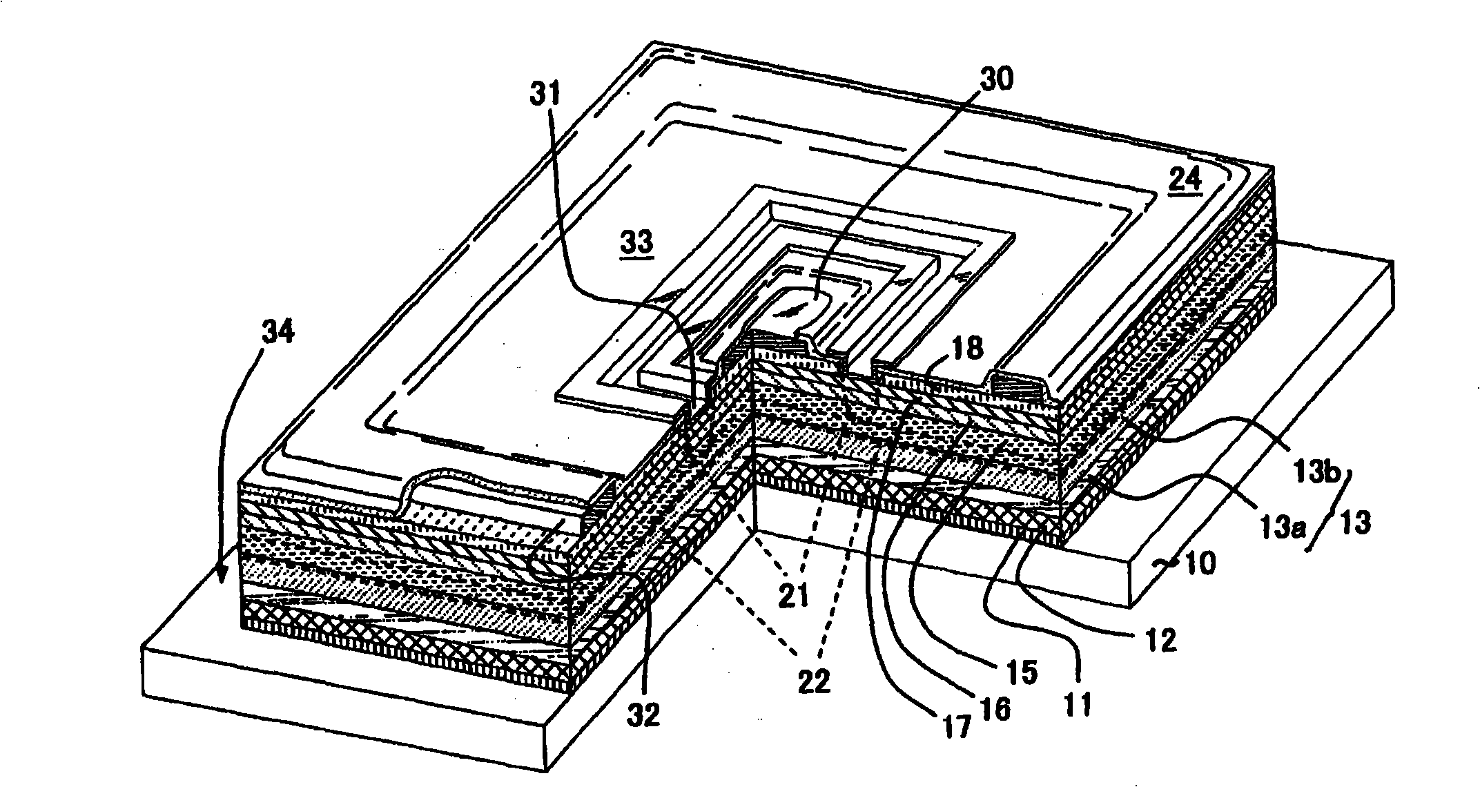
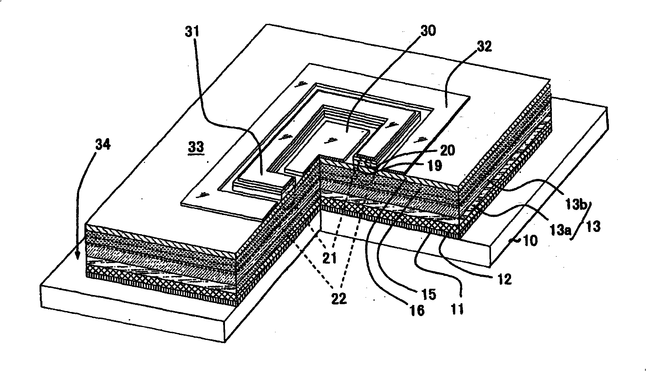
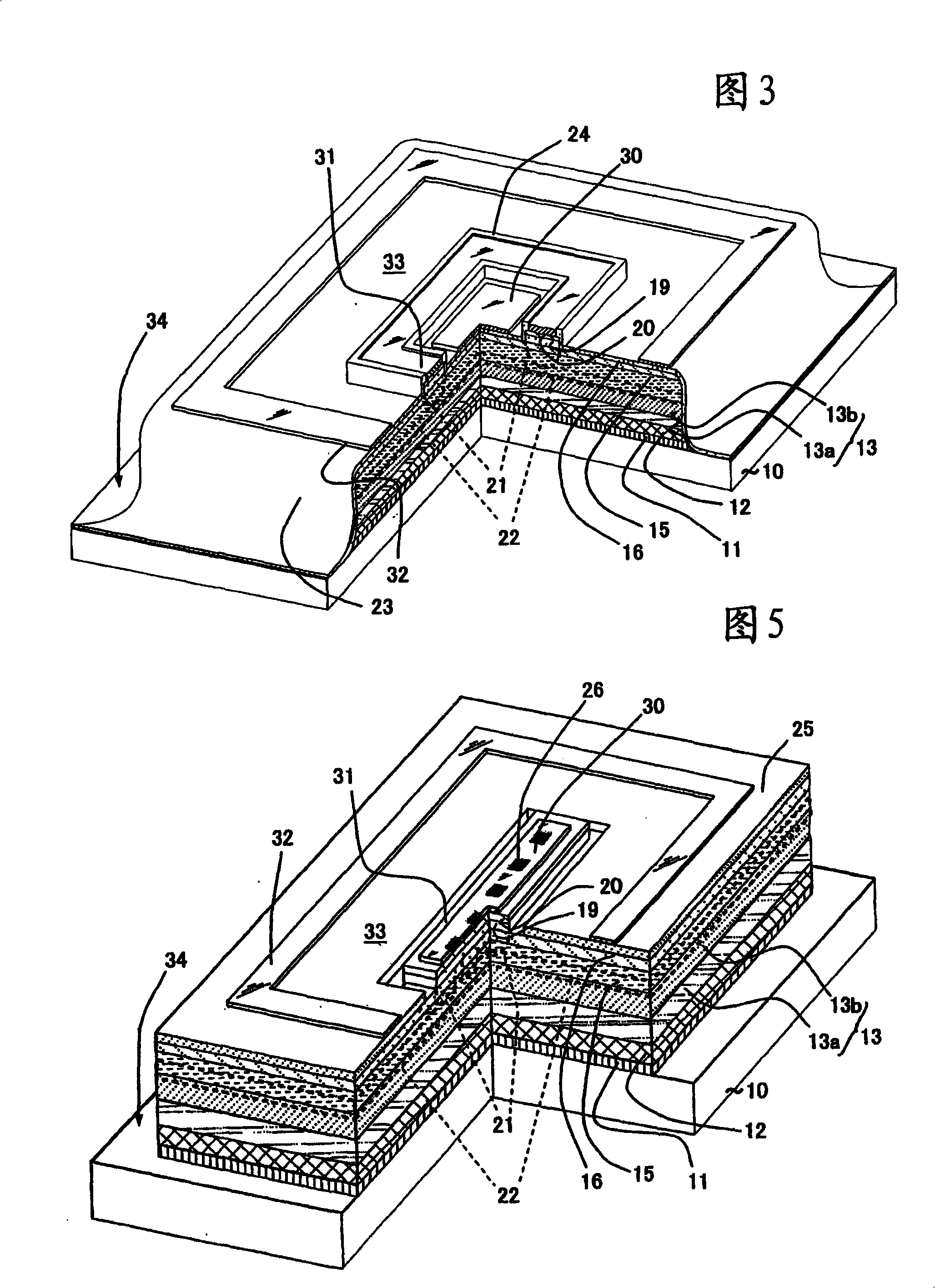
[0077] figure 1 A preferred embodiment of an optical FET with a relatively basic structure fabricated according to the invention is presented.

[0078] Generally, in long-wavelength semiconductor materials prepared by MOCVD, the background carrier concentration is n-type and about 2× 10 14 to 2×10 15 cm -3 or so, and about 1×10 in InSb-based or InAsSb-based materials used in the infrared region with wavelengths up to 6 μm 16 cm -3 about. On the other hand, in order to increase the light absorption coefficient, it is necessary to have a light absorption layer (photosensitive layer) having a thickness of at least 1 to 2 μm as a photodetector. Therefore, as a photo-control FET, in order to cut off the channel current in the dark state and obtain an amplified current corresponding to the induced charge under light, it is necessary to deplete the channel that is in t...


PUM

PropertyMeasurementUnit
wavelengthaaaaaaaaaa

Abstract

The inventive photo-FET is characterized in that a homojunction or a heterojunction is formed to a channel layer (15) between a substrate (10) and the channel layer, a substrate side depletion layer (22) is extended to the channel layer (15) from the side of the substrate (10), and layers (13; 13a, 13b) operating as both substrate side depletion layer generating layers and back gate layers are provided for performing back-gate biasing by carriers generated by irradiation of light on the channel layer (15). On the front plane side of the channel layer (15), a barrier layer (16) wherein a band gap is wider than that of the channel layer (15), one of the carriers generated by light is permitted to run on the channel layer (15) and the other carrier to stay or blocked is provided. The front side of the channel layer (15) is provided with a front side depletion layer generating layer (17) wherein a front side depletion layer (21) is extended from the front side to the channel layer (15), and an element is turned off by bringing the front side depletion layer (21) into contact with a substrate side depletion layer (22) when light is not being applied and by closing a current path inside the channel layer (15).

Description

technical field [0001] The present invention relates to improvements in photo-controlled field-effect transistors (hereinafter also referred to as photo-controlled FETs) in which a photodiode and a field-effect transistor (hereinafter also referred to as FET) are integrated in a single chip. Background technique [0002] In various applications such as medicine, disaster prevention, and industrial detection, photodetectors in the near-infrared region, especially photodetector arrays with multiple photodetectors arranged one-dimensionally or two-dimensionally, are used as spectroscopic systems or Infrared photodetectors for infrared cameras are in high demand. For example, in the fields of medicine and biometrics, non-invasive behavior has been reaffirmed and commercialized as "in vivo oxygen monitoring device" or "vessel image authentication device" that utilizes the spectral characteristics of hemoglobin between 0.7 and 0.9 μm in the near-infrared region. system". The sco...

Claims


Application Information

Patent Timeline
Patent Type & Authority Applications(China)
IPC IPC(8): H01L31/10H01L21/28H01L21/337H01L29/66H01L29/80H01L29/808
CPCH01L27/14603H01L27/14643H01L31/10H01L29/80H01L29/808
Inventor 小仓睦郎
Owner NAT INST OF ADVANCED IND SCI & TECH
Why Eureka
Try Eureka