Apparatus for ordered adhering various cells to setting position of same substrate and adhesion method
A technology for setting position and cells, applied in biochemical equipment and methods, immobilized enzymes, microbial measurement/testing, etc., can solve the problem of cell patterns that cannot interact, operate complicatedly, and cannot control adhesion well Sports and other issues
- Summary
- Abstract
- Description
- Claims
- Application Information
AI Technical Summary
Problems solved by technology
Method used
Image
Examples
Embodiment 1
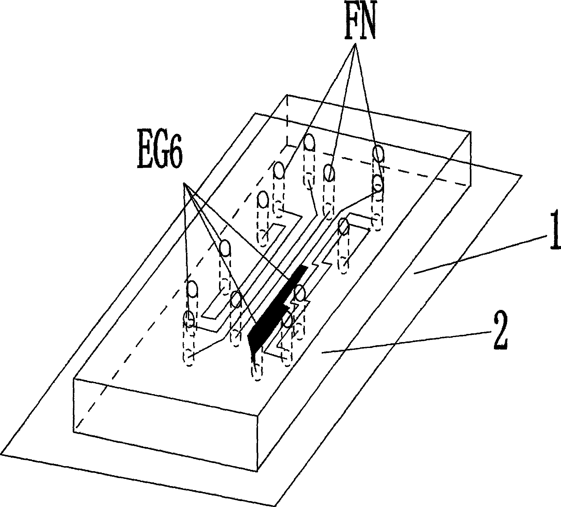
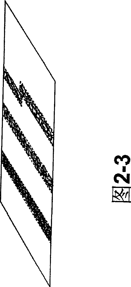
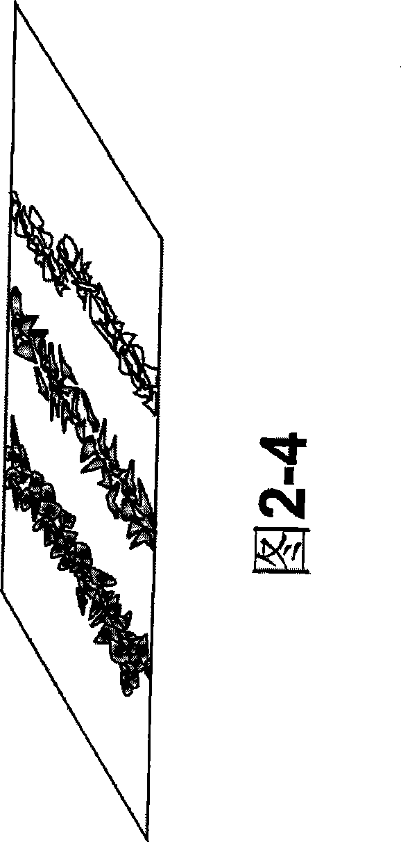
[0078] Please refer to Figure 2-1, Figure 2-2, Figure 2-3 and Figure 2-4:
[0079] 1) Evaporate a 10nm (2-10nm) titanium adhesion layer on the surface of a clean glass slide 1 (thickness 0.15mm), and then vapor-deposit a 40nm (20-50nm) titanium adhesion layer on the surface Thick gold layer, making substrate 1;
[0080] Cut the prepared substrate 1 into 2 x 2cm 2 Soak the small pieces in an aqueous solution of ethanol (concentration: 50% to 100%), then blow dry with nitrogen for subsequent use;
[0081] 2) Use photolithography technology to engrave a pattern with at least one group of convex strip microstructure units on a silicon wafer. The manufacturing steps are as follows: first use the drawing software L-edit to design seven parallel convex strips of the desired pattern. Shaped lines, the seven parallel convex lines form a set of convex strip microstructure units, including:
[0082] Straight-line central convex strip in the middle position;
[0083] The first convex ...
Embodiment 2
[0091] 1) Evaporate a 5nm (2-10nm) chrome adhesion layer on the surface of a clean glass slide (thickness 0.15mm), and then vapor-deposit a 20nm (20-50nm) thickness on the chromium adhesion layer The gold layer is made substrate 1;
[0092] Cut the prepared substrate 1 into 2 x 2cm 2 Soak the small pieces in an aqueous solution of ethanol (concentration: 50% to 100%), then blow dry with nitrogen for subsequent use;
[0093]2) Use photolithography technology to engrave a pattern with at least one group of convex strip microstructure units on a silicon wafer. The manufacturing steps are as follows: first use the drawing software L-edit to design seven parallel convex strips of the desired pattern. Shaped lines, the seven parallel convex lines form a set of convex strip microstructure units, including:
[0094] Straight-line central convex strip in the middle position;
[0095] The first convex strip, the second convex strip and the third convex strip arranged in sequence on o...
Embodiment 3
[0103] The substrate obtained in embodiment 1 or embodiment 2 that has been adhered to various cells is immersed in common cell culture fluid (fetal bovine serum concentration 10%); a positive electrode is connected to the solution, and a negative electrode is connected to the gold surface of the thiolated substrate , the voltage is 1.4V, the power-on time is 30s, and an electrochemical analysis is performed once. The thiol analysis and attachment of the gold surface area outside the specified pattern becomes the surface layer that can adsorb proteins and cells again, and adheres to the specified pattern. The cells are free to move.
[0104] In addition, the convex strips of the convex strip type microstructure unit according to the present invention can also add convex strips with the same shape and parallel to the outermost convex strips as required; the microgrooves The concave grooves of the unit can also be added with the same shape and parallel concave grooves outside th...
PUM
| Property | Measurement | Unit |
|---|---|---|
| thickness | aaaaa | aaaaa |
| thickness | aaaaa | aaaaa |
| length | aaaaa | aaaaa |
Abstract
Description
Claims
Application Information


