Non-volatile memory device having a gap in the tunnuel insulating layer and method of manufacturing the same

A non-volatile storage and non-volatile technology, applied in the field of manufacturing such devices, can solve the problems of undisclosed low-k tunnel dielectric materials, mismatched semiconductor manufacturing processes, and reduced reliability of storage devices, and achieve improved Effect of charge retention time, improved reliability and data retention time, and reduced leakage current

Inactive Publication Date: 2009-02-25
NXP BV
View PDF2 Cites 8 Cited by
  • Summary
  • Abstract
  • Description
  • Claims
  • Application Information

AI Technical Summary

Problems solved by technology

However, this document does not disclose suitable low-k tunnel dielectric materials
Furthermore, the practical application of high-k materials has profound disadvantages, such as diff

Method used


Image

  • Non-volatile memory device having a gap in the tunnuel insulating layer and method of manufacturing the same
  • Non-volatile memory device having a gap in the tunnuel insulating layer and method of manufacturing the same
  • Non-volatile memory device having a gap in the tunnuel insulating layer and method of manufacturing the same

Examples


Embodiment Construction

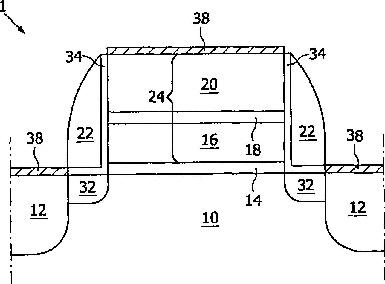
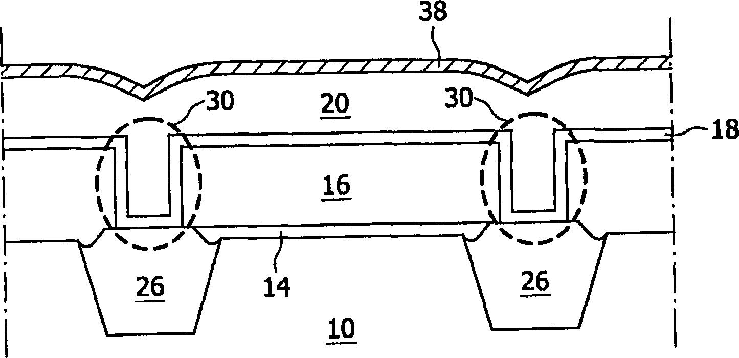
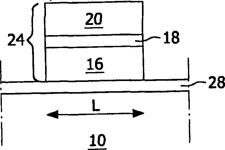
[0044] According to the invention, in a first step, a substrate is provided. In embodiments of the present invention, the term "substrate" includes any underlying material or material on which devices, circuits or layers may or have been formed. Examples of semiconductor substrates are: doped silicon, gallium arsenide (GaAs), gallium arsenide phosphide (GaAsP), germanium (Ge) or silicon germanium (SiGe). The substrate may include, for example, silicon dioxide or silicon nitride other than the semiconductor substrate portion. Thus, the term substrate also includes: silicon on insulator, silicon on glass (SOG), silicon on sapphire (SOS) and silicon on any material (SOA). Thus, the term substrate is used to broadly define a layer serving as a basis for a layer or portion of interest. Furthermore, the substrate may be any basis on which a layer is formed, for example a glass or metal layer. Also it should be pointed out that the substrate need not have a flat surface.

[0045]...


PUM


Abstract

A non- volatile memory device (1, 101, 201, 301) having a gap within a tunnel dielectric layer (14, 114, 214, 314) and a method of manufacturing the same is provided. The devices have a stack of layers on top of a substrate (10, 110, 210, 310) including, a charge tunneling layer with a gap (14, 114, 214, 314), a charge storage layer (16, 116, 216, 316), a control gate layer (20, 120, 220, 320) and an insulating layer (18, 118, 218 220) in between the charge storage layer and the control gate. Manufacturing proceeds through deposition of a sacrificial layer (28, 128,228,328) on parts of a substrate, whereupon a stack of layers (24, 124,224,324) including a charge-storage layer, an insulating layer and a control gate layer are formed. Subsequently, selected parts of the sacrificial layer are removed, thereby forming a gap in between the charge storage region and the substrate. The gap is protected from future processing by deposition of a sealing layer (34, 134, 234, 334). Such a device has a reduced operating voltage and its manufacture can be easily implemented in existing semiconductor processes.

Description

technical field [0001] The present invention relates to non-volatile memory devices and devices including such devices. Such devices can be used as stand-alone or embedded non-volatile memory (NVM), such as electrically erasable programmable read-only memory (EEPROM) or flash memory. The invention also relates to methods of making such devices. Background technique [0002] A non-volatile memory device typically consists of a transistor device comprising a source region, a drain region and a channel between the drain and source regions formed in a silicon semiconductor substrate region, and a charge storage region (CSR) formed on the substrate between the channel region and a conductive control gate, usually made of highly doped polysilicon. The charge storage region is separated and insulated from the substrate by a tunnel dielectric layer and from the control gate by an insulating layer. [0003] In conventional devices, the CSR consists of a floating gate made of heavi...

Claims


Application Information

Patent Timeline
IPC IPC(8): H01L21/28H01L21/336H01L21/8247H01L21/84H01L27/115H01L27/12H01L29/788H01L29/792H01L29/423H01L29/51
CPCH01L29/785H01L29/66825H01L27/11521H01L29/66833H01L27/11568H01L21/28282H01L29/792H01L29/66795H01L21/84H01L29/7883H01L27/115H01L21/28273H01L27/1203H01L29/40114H01L29/40117H10B43/30H10B69/00H10B41/30
Inventor 罗伯图斯·T·F·范沙吉克迈克尔·J·范杜里恩
Owner NXP BV
Why Eureka
Try Eureka